

Polarizing device and laser unit
a polarizing device and laser unit technology, applied in the direction of polarizing elements, instruments, optics, etc., can solve the problems of complex inability to obtain the circular cross section of the radial polarized light beam, and high cost so as to achieve the effect of low cost and simple configuration of the polarizing devi
- Summary
- Abstract
- Description
- Claims
- Application Information
AI Technical Summary
Benefits of technology
Problems solved by technology
Method used
Image

Examples
Embodiment Construction
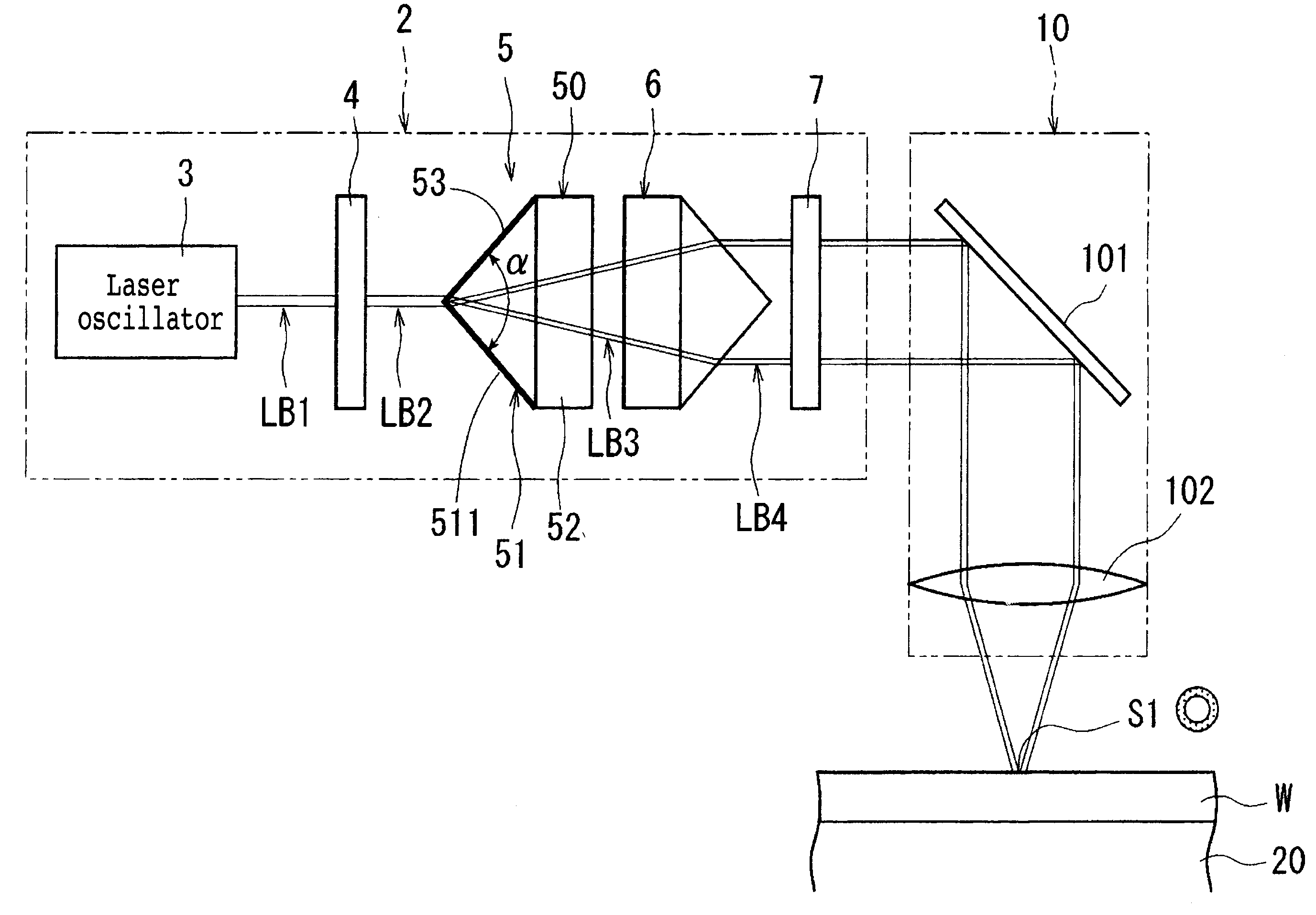
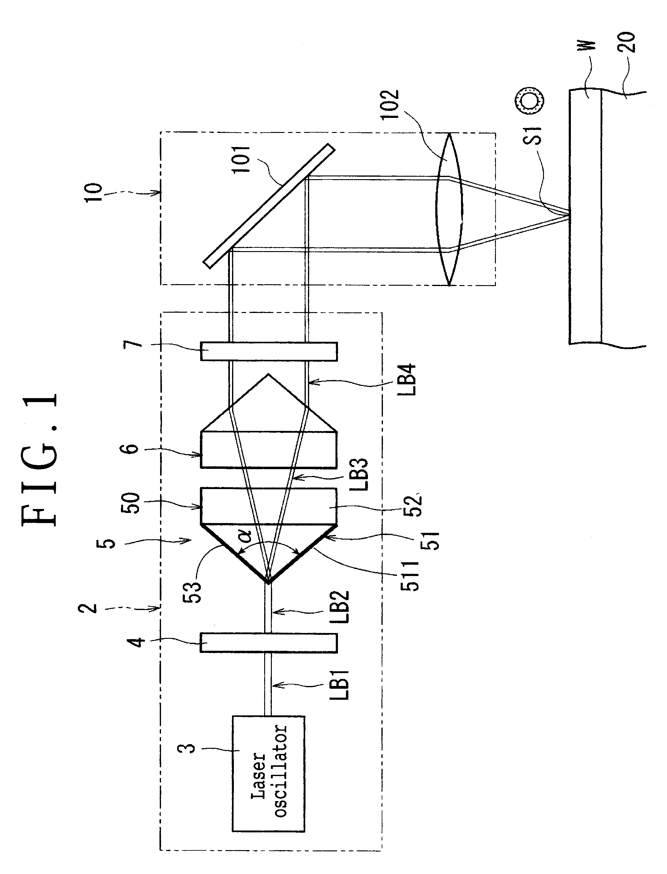
[0020]Some preferred embodiments of the present invention will now be described in detail with reference to the attached drawings. FIG. 1 shows a laser processing apparatus including a laser unit 2 using a polarizing device 5 according to a first preferred embodiment of the present invention. The laser processing apparatus shown in FIG. 1 is composed of the laser unit 2 and a focusing apparatus 10 for focusing a laser beam applied from the laser unit 2 onto a workpiece W held on a chuck table 20.
[0021]The laser unit 2 shown in FIG. 1 includes a laser oscillator 3, a quarter-wave plate 4, the polarizing device 5 according to this preferred embodiment, an axicon lens 6, and a half-wave plate 7 arranged in series in this order in the propagation direction of light. The laser oscillator 3 oscillates a linearly polarized light beam LB1. The quarter-wave plate 4 converts the linearly polarized light beam LB1 oscillated from the laser oscillator 3 into a circularly polarized light beam LB2...
PUM
 Abstract
Description
Claims
Application Information