Method of manufacturing photoelectric conversion device

a technology of photoelectric conversion and manufacturing method, which is applied in the manufacture of final products, sustainable manufacturing/processing, electrochemical generators, etc., can solve the problems of long occupation time and difficulty in selective coloring with dyes, and achieve the effect of selective dye adsorption

Inactive Publication Date: 2010-06-10
SONY CORP
View PDF26 Cites 14 Cited by
  • Summary
  • Abstract
  • Description
  • Claims
  • Application Information

AI Technical Summary

Benefits of technology

[0020]As described above, according to one aspect of the prese

Problems solved by technology

However, with the conventional techniques including Patent Document 1, it is difficult to perform selective coloring with dye

Method used


Image

  • Method of manufacturing photoelectric conversion device
  • Method of manufacturing photoelectric conversion device
  • Method of manufacturing photoelectric conversion device

Examples


first embodiment

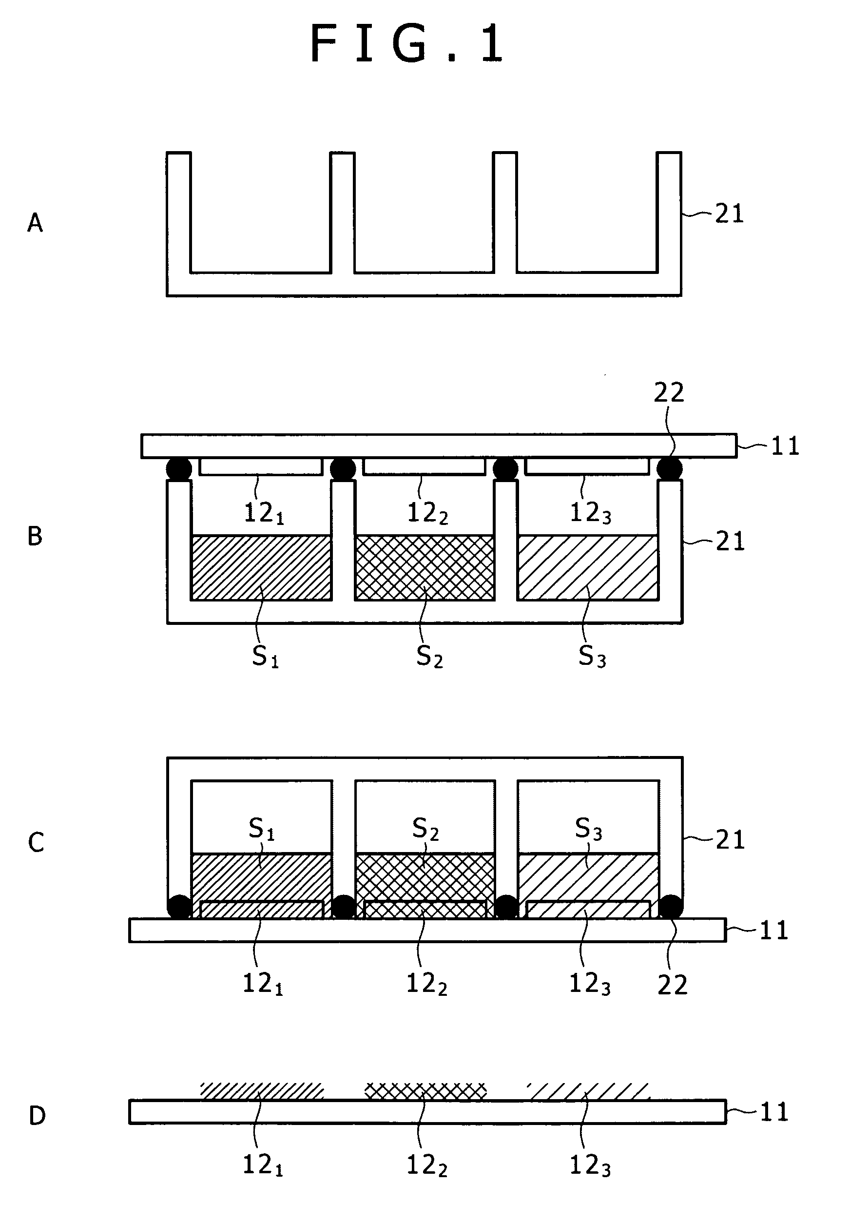
[0039]The steps (1), (2), and (3) as a stage preceding the (4) dye adsorbing process coat a commercial FTO glass (15 Ω / □) with a commercial TiO2 paste by a screen printing process, and sinter the FTO glass for one hour at 500° C. Thus, a titanium oxide electrode (average film thickness of 20 μm) having a strip-shaped pattern is obtained.

[0040]The process next proceeds to the (4) dye adsorbing process. The process represented in a sectional view of the step of the (4) dye adsorbing process of FIG. 1 is performed. Incidentally, in FIG. 1, the strip-shaped titanium oxide electrode obtained in the steps of (1) to (3) is described as semiconductor electrodes 121 to 123.

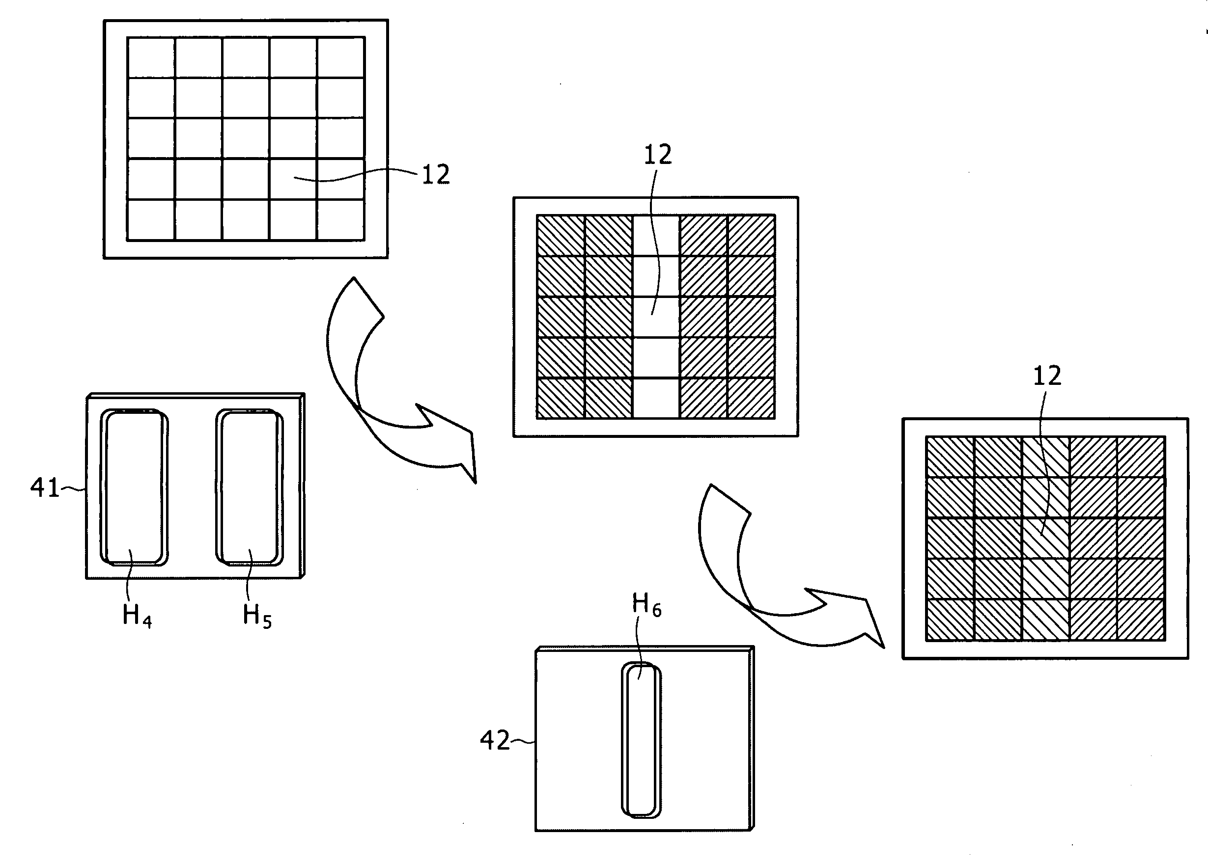
[0041]As shown in A of FIG. 1, a material unit 21 is of a container shape (tray shape) having a bottom part. In addition, the material unit 21 has partition walls of a predetermined shape. Different dye solutions can be put in respective sections divided by the partition walls. For example, in A of FIG. 1, the material uni...

second embodiment

[0050]In the foregoing [First Embodiment], an example of using the adhesive 22 and an example of press-fitting by a gasket have been described as the method of laminating the material unit 21. However, the press-fitting method includes not only a mechanical press-fitting method but also a press-fitting method using atmospheric pressure such as laminating the material unit 21 in a vacuum and then returning the material unit 21 to atmospheric pressure.

[0051]Specifically, a material unit 21 that has partition walls in which three kinds of dye solutions S1 to S3 similar to those of [First Embodiment] are injected and which is provided with a silicon rubber layer on the outer circumferences of the partition walls is mechanically laminated to semiconductor electrodes 121 to 123 fabricated by a similar method to that of [First Embodiment] (steps (1) to (3)). Thereafter, the internal space of the material unit 21 set in a sealed state by being laminated is decompressed by a vacuum pump, whe...

third embodiment

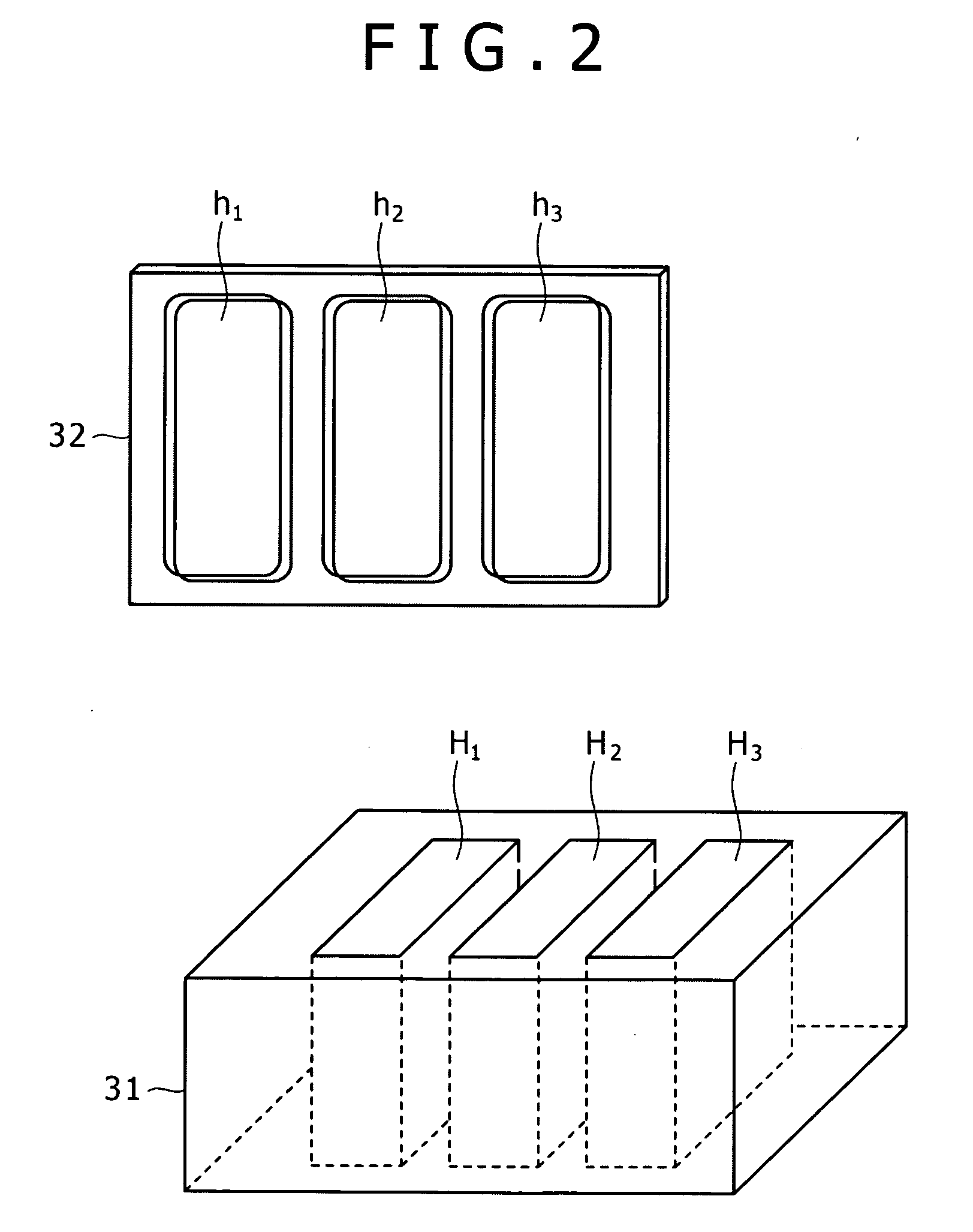
[0053]In the foregoing [First Embodiment], description has been made of a constitution in which dyes are adsorbed on the semiconductor electrodes 121 to 123 by inverting the material unit 21 in FIG. 1. However, dyes can be adsorbed without the member being inverted by using a material unit 31 in FIG. 2. Incidentally, in FIG. 2, a diagram on a lower side is a perspective view of the material unit 31, and a diagram on an upper side is a top view of a silicon rubber 32.

[0054]Specifically, the material unit 31 having a hollow shape is mechanically press-fitted to semiconductor electrodes 121 to 123 fabricated by a similar method to that of [First Embodiment] (steps (1) to (3)) via the silicon rubber 32 having hole parts h1 to h3 corresponding to the hollow parts H1 to H3 of the material unit 31. That is, at this time, the semiconductor electrodes 121 to 123 are situated at the bottom part of the material unit 31 having the hollow shape. Thereafter, when three kinds of dye solutions S1 t...


PUM


Abstract

The present invention relates to a method of manufacturing a photoelectric conversion device in which selective dye adsorption can be performed easily. In the step of a dye adsorbing process, a material unit 21 having partition walls of a predetermined shape is placed over semiconductor electrodes 121 to 123, which are a titanium oxide electrode. The material unit 21 is laminated by a UV cure adhesive. Dye solutions S1 to S3 obtained by dissolving each of three kinds of dyes of N719, Black dye, and D149, for example, into a CH3CN/t-BuOH mixed solution are put in each of sections divided by the partition walls. The material unit 21 is inverted in that state, and left standing still for 24 hours. Then, the adhesive is removed after passage of the 24 hours. Thus, the semiconductor electrodes 121 to 123 having regions corresponding to the sections which regions are colored with the three different kinds of dyes are obtained. The present invention is applicable to a method of manufacturing a dye sensitized solar cell.

Description

TECHNICAL FIELD[0001]The present invention relates to a method of manufacturing a photoelectric conversion device, and particularly to a method of manufacturing a photoelectric conversion device in which selective dye adsorption can be performed easily.BACKGROUND ART[0002]Researches into dye sensitized solar cells as next-generation solar cells to replace a silicon (Si) type have recently been conducted widely.[0003]The dye sensitized solar cell has features including an easy manufacturing process and an ability to be provided with design quality. As an example of design quality, a solar cell having a plurality of colors would be able to be installed without impairing the external appearance of an apparatus, an electronics device, a building or the like on which to install the solar cell, which is considered to lead to further spread of solar cells.[0004]As for applications, the dye sensitized solar cell may be applied to for example power supplies of various electronics devices suc...

Claims


Application Information

Patent Timeline
IPC IPC(8): H01L31/18
CPCH01G9/2031H01G9/2063Y02E10/542H01G9/2072H01M14/005H01G9/2068Y02P70/50
Inventor SUZUKI, YUSUKEMOROOKA, MASAHIROTADA, KEISHINAGANO, YASUNORIYONEYA, REIKOORIHASHI, MASAKITAKADA, HARUMIZHU, CHENG
Owner SONY CORP
Why Eureka
Try Eureka