Method of forming a MOS transistor

a technology of mos transistor and mos, which is applied in the direction of transistors, electrical devices, basic electric elements, etc., can solve the problems of reducing access resistance, difficult control of junction depth, and reducing access resistance, so as to improve the short channel effect, the effect of co-existing dopants and good junction profil

Active Publication Date: 2010-06-10
MARLIN SEMICON LTD
View PDF58 Cites 8 Cited by
  • Summary
  • Abstract
  • Description
  • Claims
  • Application Information

AI Technical Summary

Benefits of technology

[0014]The method of forming a MOS transistor comprises a step of co-implantation to implant a carbon co-implant from a precursor comprising CO or CO2 within substantially the same place as that of the lightly doped drain or source, the source region and the drain region, or the halo implanted region. Therefore, after a rapid thermal process is performed, for example, by a conventional ...

Problems solved by technology

With the device scaling down, it's difficult to control the junction depth (Xj) and also reduce the access resistance.
But from 65 nm node and beyond, the conventional As (arsenic) ...

Method used


Image

  • Method of forming a MOS transistor
  • Method of forming a MOS transistor
  • Method of forming a MOS transistor

Examples


Embodiment Construction

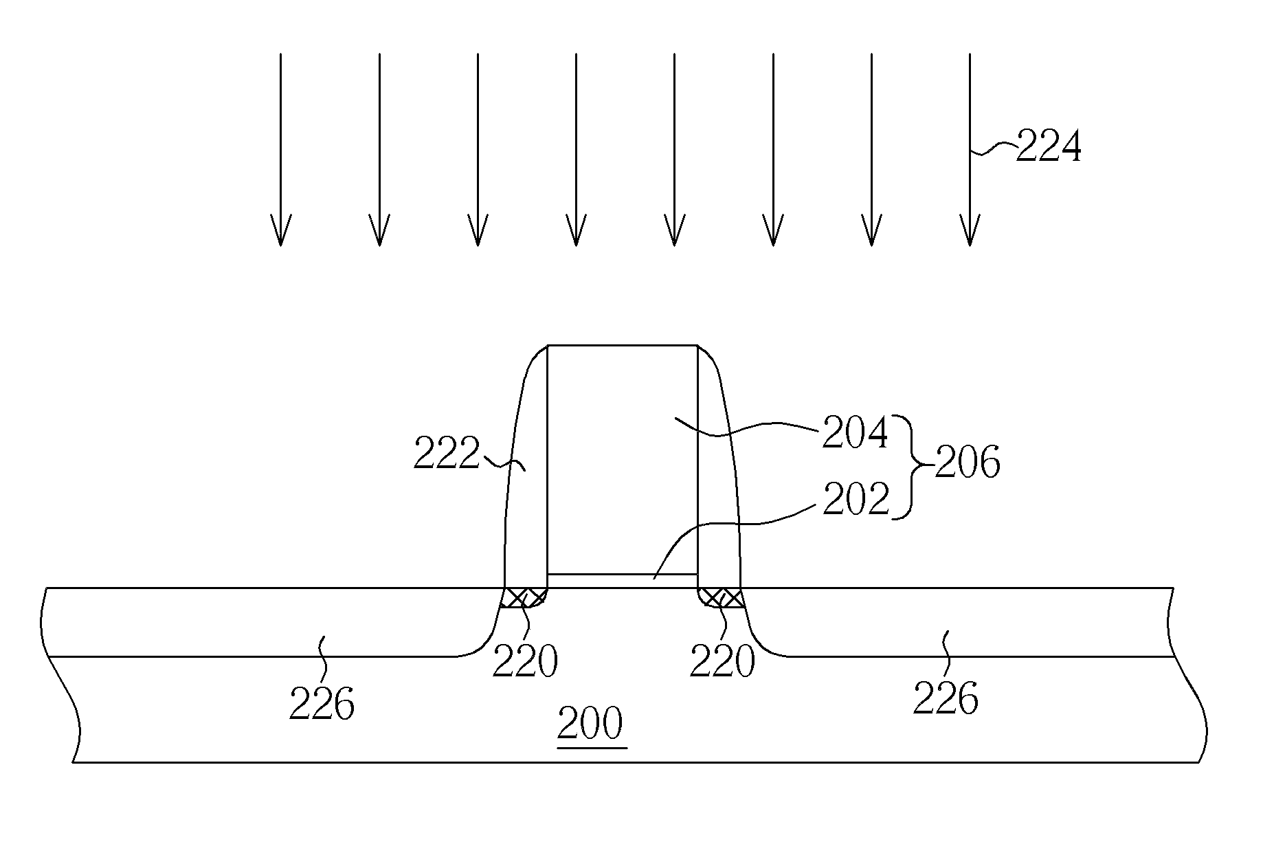
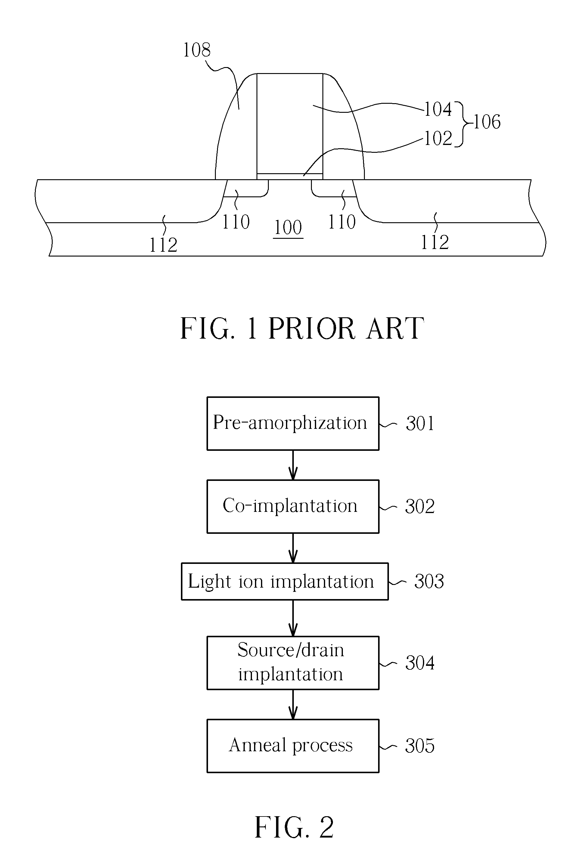
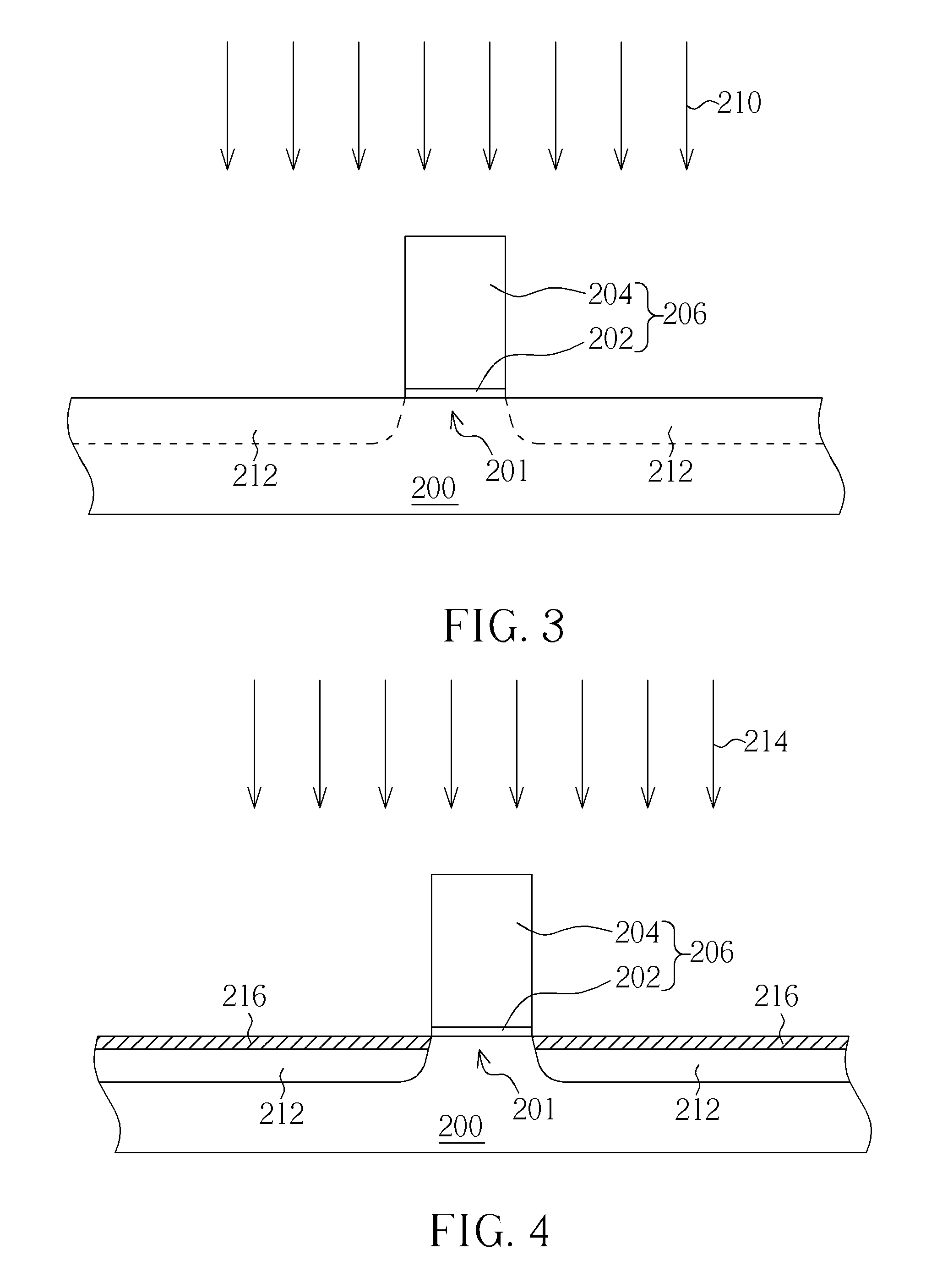
[0024]Refer to FIGS. 2 to 6 for illustration of an embodiment according to the present invention. FIG. 2 is a flow chart showing the method of forming a MOS transistor according to the present invention. The method of forming a MOS transistor of the embodiment according to the present invention comprises the steps as follows. A substrate having a gate, a source region and a drain region, and a channel region is provided. A pre-amorphization 301 is performed to form an amorphized region in the source region and the drain region, respectively. A co-implantation 302 is performed to implant a carbon co-implant within the source region and the drain region. A light ion implantation 303 is performed to form a doped region in the source region and the drain region. A spacer is formed on the sidewall of the gate. A source / drain ion implantation 304 is performed to form a doped region. An anneal process 305 is performed to activate the dopants, regrow the amorphized regions to a substantiall...


PUM


Abstract

A method of forming a MOS transistor, in which, a co-implantation is performed to implant a carbon co-implant into a source region and a drain region or a halo implanted region to effectively prevent dopants from over diffusion in the source region and the drain region or the halo implanted region, for obtaining a good junction profile and improving short channel effect, and the carbon co-implant is from a precursor comprising CO or CO2.

Description

CROSS REFERENCE TO RELATED APPLICATIONS[0001]This is a continuation-in-part of U.S. application Ser. No. 12 / 127,787 filed on May 27, 2008, which is a continuation-in-part of U.S. application Ser. No. 11 / 278,434 filed on Apr. 3, 2006, now U.S. Pat. No. 7,396,717, and both are included herein by reference.BACKGROUND OF THE INVENTION[0002]1. Field of the Invention[0003]The present invention relates to a method of forming a MOS transistor, and particularly to a method of forming a MOS transistor having an improved short channel effect.[0004]2. Description of the Prior Art[0005]Field effect transistors (FETs) are important electronic devices in the fabrication of integrated circuits, and as the size of the semiconductor device becomes smaller and smaller, the fabrication of the transistors is also improved and constantly enhanced for fabricating transistors with smaller sizes and higher quality.[0006]In the conventional method of fabricating transistors, a gate structure is first formed ...

Claims


Application Information

Patent Timeline
IPC IPC(8): H01L21/265
CPCH01L21/26506H01L29/6659H01L21/26586H01L21/26513
Inventor WANG, HSIANG-YINGCHIEN, CHIN-CHENGHSIAO, TSAI-FUCHIEN, MING-YENCHEN, CHAO-CHUN
Owner MARLIN SEMICON LTD
Why Eureka
Try Eureka