Automated semiconductor design flaw detection system

a technology of automatic detection and semiconductors, applied in the field of automatic detection of semiconductor design flaws, can solve the problems of not providing any mechanism to compare the differences between physical and logical designs, logic simulators by themselves provide no information to compare realized physical implementation, and commercially available lvs tools

Active Publication Date: 2010-06-10
ALTERA CORP
View PDF18 Cites 66 Cited by
  • Summary
  • Abstract
  • Description
  • Claims
  • Application Information

AI Technical Summary

Benefits of technology

[0013]Logic simulators by themselves provide no information to compare realized physical implementation against simulation models that produce them. Nor do logic simulators provide any mechanism to compare the differences between physical and logical designs. I

Problems solved by technology

Logic simulators by themselves provide no information to compare realized physical implementation against simulation models that produce them.
Nor do logic simulators provide any mechanism to compare the differences between physical and logical designs.
In ad

Method used


Image

  • Automated semiconductor design flaw detection system
  • Automated semiconductor design flaw detection system
  • Automated semiconductor design flaw detection system

Examples


Embodiment Construction

[0036]A description of example embodiments of the invention follows.

[0037]The steps and processes below are described in the context of FPGA design flows. Those skilled in the art will recognize that these processes and concepts apply to other areas such as application specific integrated circuit (ASIC) and software design, as well as design and implementation of other semiconductor devices.
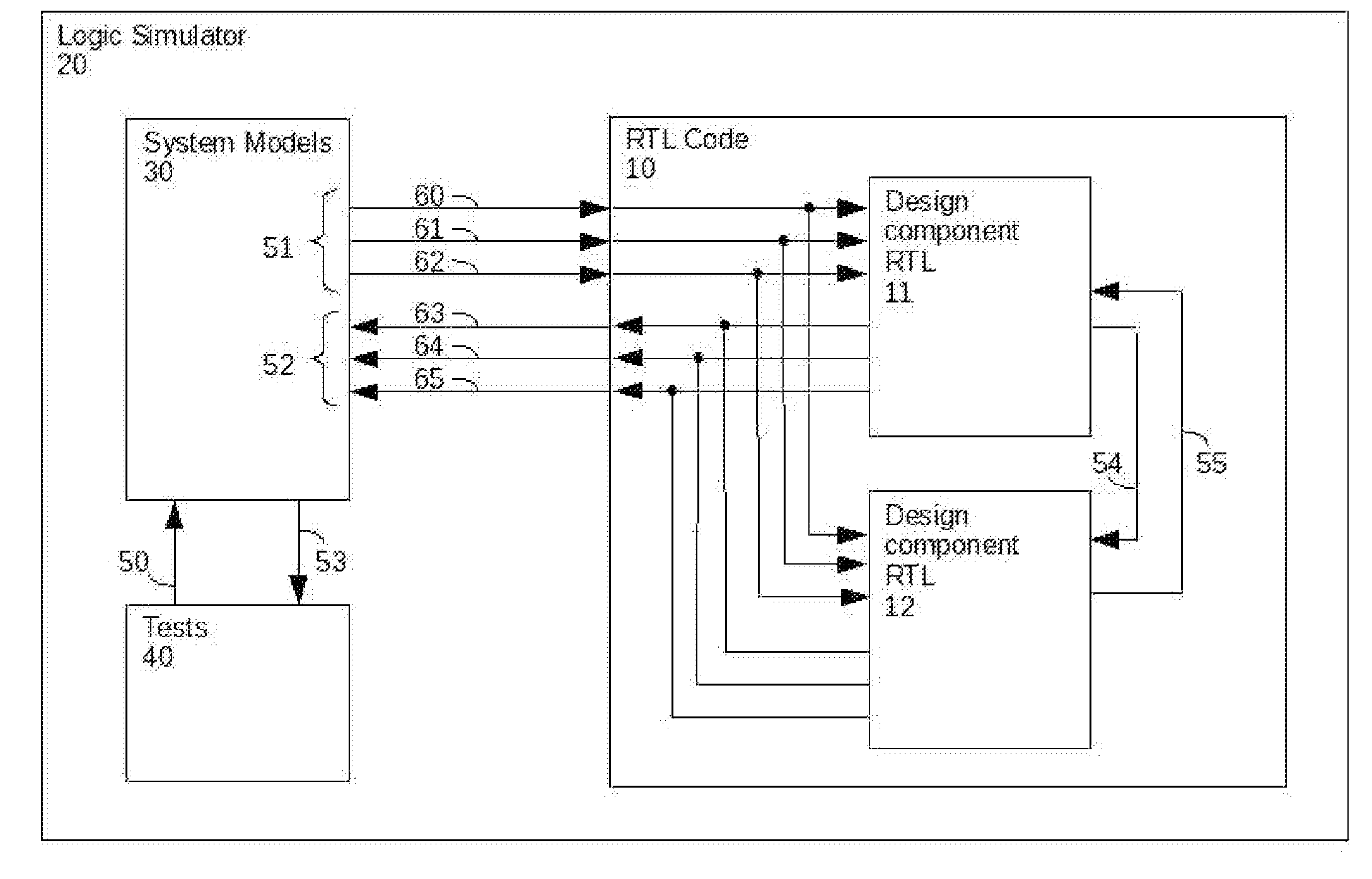
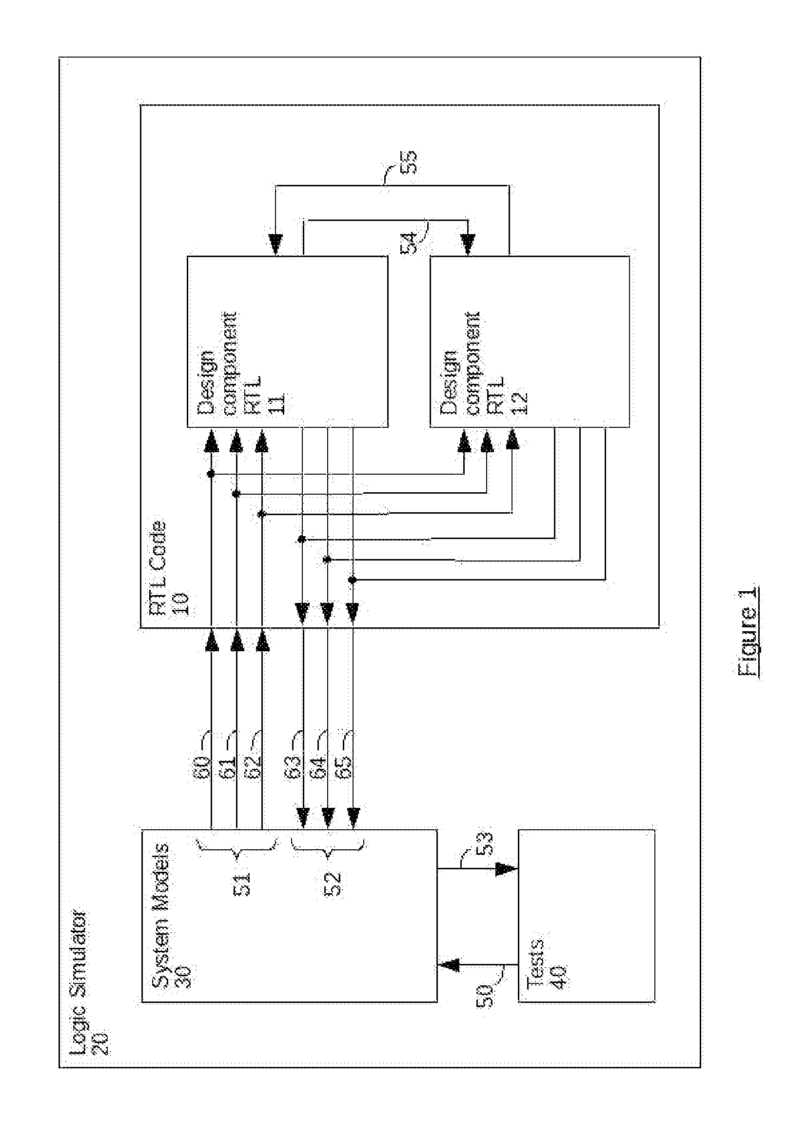
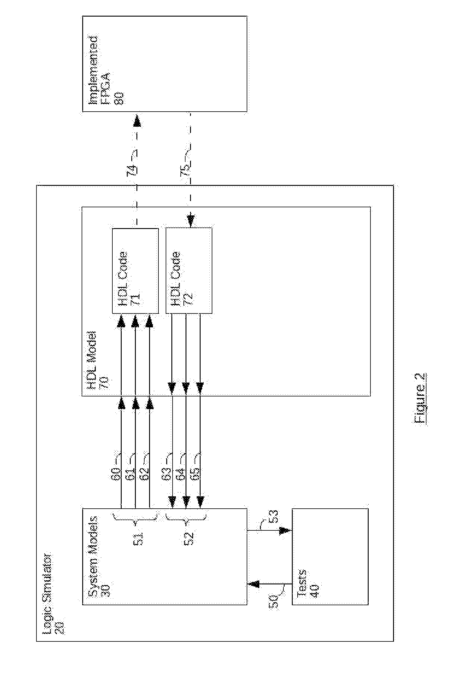
RTL Coding

[0038]The register transfer level (RTL) coding process involves hand-crafting code that captures the intent of the hardware designer. Coding is a manual process and thus error prone. Furthermore, RTL, being a hardware description language (HDL), is subject to interpretation by those writing the code and software tools that consume it. Perfect alignment of language interpretation is required to avoid introduction of inadvertent behavior in hardware designers' code.

[0039]The implications of misaligned HDL interpretation manifest as divergent behavior between intended design function and a...


PUM


Abstract

The process by which a logical simulation model is implemented in a physical device may introduce errors in the resulting implementation. A simulation system enables comparison of a realized physical implementation against the simulation models that produce them, thereby detecting differences between an initial, logical design and the resulting physical embodiment. Errors introduced by an initial design, faulty Intellectual Property blocks, faulty programmable logic device silicon, faulty synthesis algorithms and software, and faulty place and route algorithms and software may be detected. As a result, the simulation system reflects both the accuracy of the actual implemented device with the capacity and performance of a purpose built hardware-assisted solution.

Description

RELATED APPLICATION(S)[0001]This application claims the benefit of U.S. Provisional Application No. 61 / 201,028, filed on Dec. 5, 2008. The entire teachings of the above application are incorporated herein by reference.BACKGROUND OF THE INVENTION[0002]Programmable logic devices are used for a wide variety of custom hardware development. These devices contain configurable logic and circuits that can be programmed to implement a wide range of custom hardware designs and functions.[0003]The configurable logic circuits are made up of a sea of primitive digital and analog elements that can selectively be wired to each other to implement a desired function.[0004]Programmable logic devices are commonly known by the acronyms “CPLD” (complex programmable logic device) and “FPGA” (field programmable gate array). CPLDs are smaller devices, capable of selecting 10's or 100's of individual logical and / or electrical elements. FPGAs are typically larger devices capable of implementing 10's of thous...

Claims


Application Information

Patent Timeline
IPC IPC(8): G06F11/00G06F17/50
CPCG06F11/3648G06F11/3656G06F2217/86G06F11/3692G06F17/5054G06F11/3664G06F13/22G06F30/34G06F2117/08G06F30/33G06F30/331G06F30/3308G06F30/347
Inventor SCHALICK, CHRISTOPHER A.SULLIVAN, JR., RODERICK B.MEDNICK, ELLIOTT H.KOPSER, MATTHEW D.
Owner ALTERA CORP
Why Eureka
Try Eureka