Unlock instant, AI-driven research and patent intelligence for your innovation.
Capacitor-equipped semiconductor device
Inactive Publication Date: 2010-06-17
PANASONIC CORP
View PDF0 Cites 7 Cited by
Summary
Abstract
Description
Claims
Application Information
AI Technical Summary
This helps you quickly interpret patents by identifying the three key elements:
Problems solved by technology
Method used
Benefits of technology
Benefits of technology
[0016]In this structure where the sheet-like substrate having a capacitor is interposed between the semiconductor chip and the mounting substrate, the height of the semiconductor device can be the same as in the conventional structures. This results in a slim and compact semiconductor device with a built-in capacitor for noise prevention.
[0017]Furthermore, the sheet-like substrate having the film capacitor thereon is produced separately from the mounting substrate, thereby providing a simple production process simple and a high yield. These components can be inspected to use only the non-defective ones so as to improve the yield of the semiconductor device, thereby producing inexpensive semiconductor devices.
Problems solved by technology
However, attaching the chip capacitor to the circuit board requires a long wire length between the semiconductor chip and the chip capacitor.
This reduces the noise absorbing performance and hence degrades the performance as a decoupling capacitor.
This results in the minimization of the wire length between the semiconductor chip and the capacitor.
Moreover, forming the capacitors, throughholes, wiring patterns, and the like on the insulation base material makes the production process complicated and makes it difficult to obtain a high yield.
As a result, the interposer of Patent Document 2 also requires a complicated production process and the yield is low.
In Patent Documents 1 and 2, the capacitors are built in the interposer; however, the process of producing the interposer is so complicated that the yield is low, making it impossible to produce the interposer at low cost.
When the silicon substrate on which to form the thin film capacitor is thick, the semiconductor chip may be damaged at the surface having a circuit thereon when a force is applied during flip-chip mounting.
Moreover, it is difficult to securely fill underfill resin between the semiconductor chip and the mounting substrate, thereby deteriorating the reliability.
Method used
Image
Click on the blue label to locate the original text in one second.
Reading with bidirectional positioning of images and text.
Examples
first exemplary embodiment
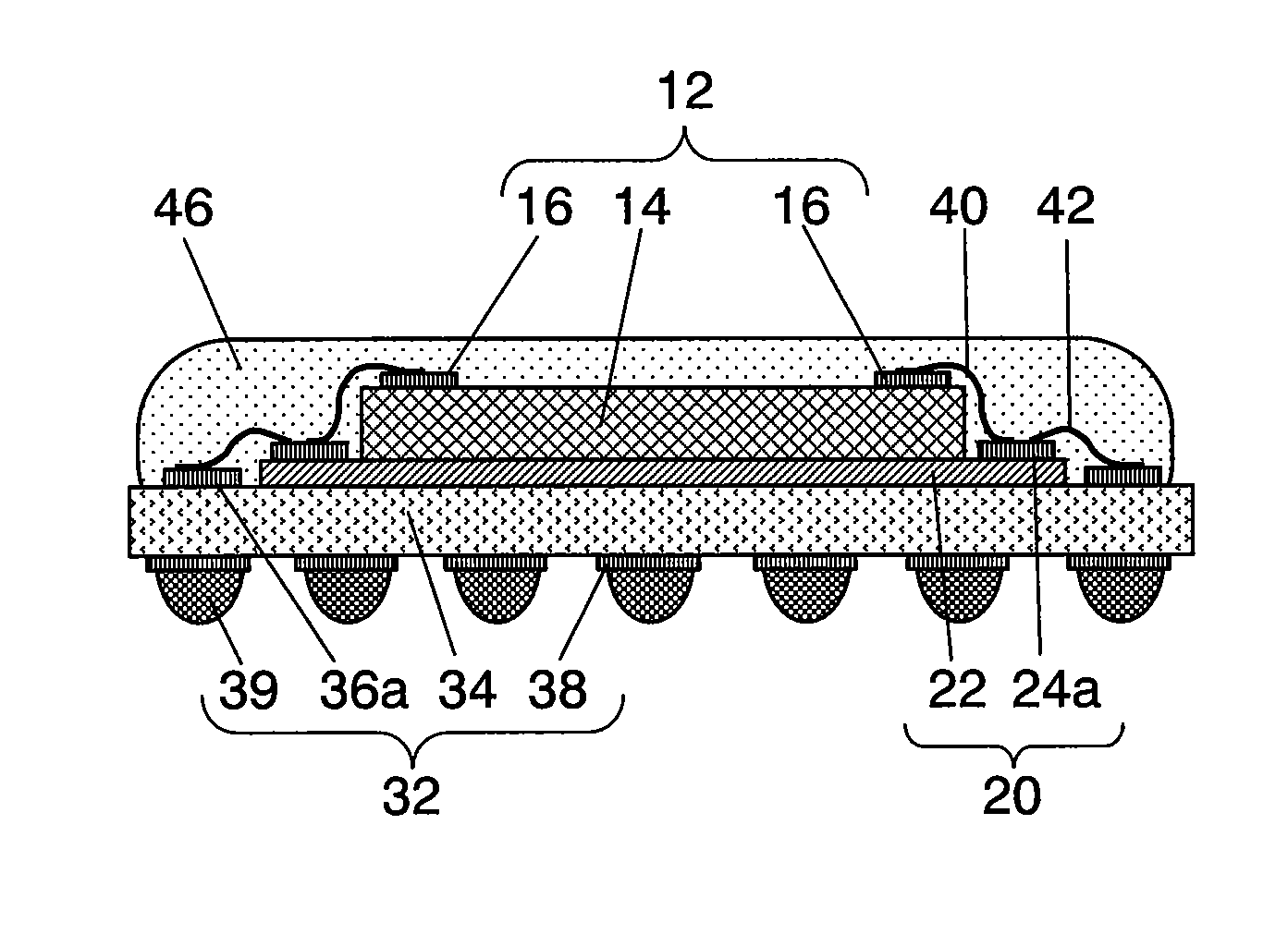
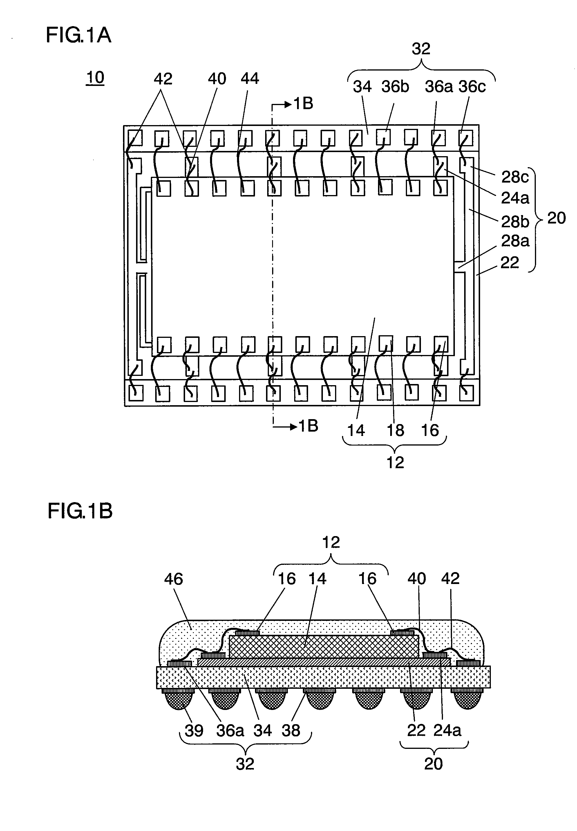
[0078]FIG. 1A is a plan view of a capacitor-equipped semiconductor device according to a first exemplary embodiment of the present invention when seen from the semiconductor chip side in a state without encapsulating resin. FIG. 1B is a sectional view taken along line 1B-1B of FIG. 1A.
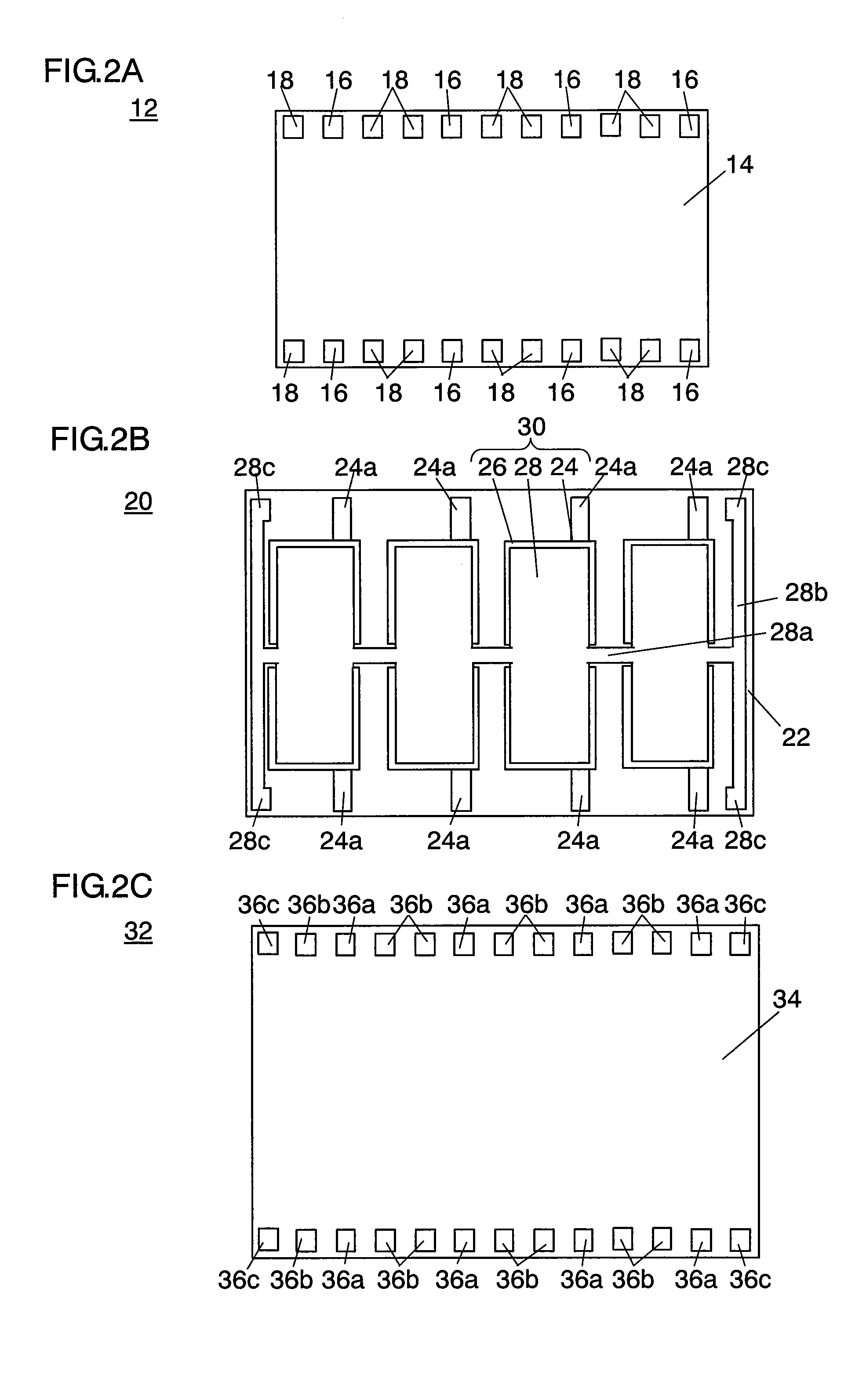
[0079]FIGS. 2A to 2C are plan views of semiconductor chip 12, sheet-like substrate 20, and mounting substrate 32, respectively, which are components of capacitor-equipped semiconductor device 10. FIG. 2A shows the semiconductor chip, FIG. 2B shows the sheet-like substrate, and FIG. 2C shows the mounting substrate.
[0080]Capacitor-equipped semiconductor device 10 of the present exemplary embodiment includes semiconductor chip 12, sheet-like substrate 20, and mounting substrate 32. Semiconductor chip 12 has a plurality of electrode terminals 16 and 18. Sheet-like substrate 20 has a plurality of film capacitors 30 formed by film forming technique. Mounting substrate 32 having external connection terminals ...
second exemplary embodiment
[0105]FIG. 6 is a sectional view of capacitor-equipped semiconductor device 50 according to a second exemplary embodiment of the present invention.
[0106]FIG. 7A is a plan view of semiconductor chip 52 of capacitor-equipped semiconductor device 50 of the present exemplary embodiment. FIG. 7B is a sectional view taken along line 7B-7B of FIG. 7A.
[0107]FIG. 8A is a plan view of sheet-like substrate 64 of capacitor-equipped semiconductor device 50 according to the present exemplary embodiment. FIG. 8B is a sectional view taken along line 8B-8B of FIG. 8A.
[0108]FIGS. 9A to 9C are plan views showing the method for producing sheet-like substrate 64 of capacitor-equipped semiconductor device 50 according to the present exemplary embodiment. FIG. 9A is a plan view of sheet base material 66 having lower electrode films 68 and the other group of electrode terminals 68a formed thereon. FIG. 9B is a plan view of sheet base material 66 having dielectric films 72 formed further thereon. FIG. 9C is...
third exemplary embodiment
[0136]FIG. 11 is a sectional view of capacitor-equipped semiconductor device 90 according to a third exemplary embodiment of the present invention.
[0137]FIG. 12 is a plan view of sheet-like substrate 100 bonded onto the surface of semiconductor chip 92 that has a circuit thereon.
[0138]FIGS. 13A to 13C are plan views showing the method for producing sheet-like substrate 100 of capacitor-equipped semiconductor device 90 according to the present exemplary embodiment. FIG. 13A is a plan view of sheet base material 102 having lower electrode films 104 and the other group of electrode terminals 104a formed thereon. FIG. 13B is a plan view of sheet base material 102 having dielectric films 106 formed further thereon. FIG. 13C is a plan view of sheet base material 102 having upper electrode films 108 and one group of electrode terminals 108a formed further thereon. The sectional view of FIG. 11 is taken along line 11-11 of FIG. 12.
[0139]Capacitor-equipped semiconductor device 90 of the pres...
PUM
Abstract
A capacitor-equipped semiconductor device includes a semiconductorchip having a plurality of electrode terminals; a sheet-like substrate at least having a film capacitor; and a mounting substrate. The mounting substrate is provided on one side thereof with chip connection terminals and ground terminals. The chip connection terminals are disposed to correspond to the electrode terminals of the semiconductor chip. The ground terminals are disposed to correspond to the one electrode terminals of the film capacitor of the sheet-like substrate. The mounting substrate is provided on the other side thereof with external connection terminals connected to the chip connection terminals and the ground terminals and used to mount the mounting substrate on an external substrate.
Description
TECHNICAL FIELD[0001]The present invention relates to a capacitor-equipped semiconductor device which has a noise reduction capacitor integrated into the package.BACKGROUND ART[0002]Conventionally, in a semiconductor device having a semiconductor chip mounted on a mounting substrate, a chip capacitor for noise reduction is attached to a circuit board on which the semiconductor device is mounted. However, attaching the chip capacitor to the circuit board requires a long wire length between the semiconductor chip and the chip capacitor. This reduces the noise absorbing performance and hence degrades the performance as a decoupling capacitor. This also prevents the miniaturization of the semiconductor device as a whole including the chip capacitor.[0003]To solve these problems, it has been tried to miniaturize semiconductor devices by providing an interposer with a built-in capacitor or by interposing an element having a capacitor function between the mounting substrate and a semicondu...
Claims
Application Information
Patent Timeline
Application Date:The date an application was filed.
Publication Date:The date a patent or application was officially published.
First Publication Date:The earliest publication date of a patent with the same application number.
Issue Date:Publication date of the patent grant document.
PCT Entry Date:The Entry date of PCT National Phase.
Estimated Expiry Date:The statutory expiry date of a patent right according to the Patent Law, and it is the longest term of protection that the patent right can achieve without the termination of the patent right due to other reasons(Term extension factor has been taken into account ).
Invalid Date:Actual expiry date is based on effective date or publication date of legal transaction data of invalid patent.

