Semiconductor die package including low stress configuration

a technology of semiconductor die and packaging, applied in the direction of semiconductor/solid-state device details, semiconductor devices, electrical equipment, etc., can solve the problems of increasing the likelihood of a package failure, stressing the semiconductor die and the molding material, and generating a significant amount of heat in the power semiconductor die packag

Active Publication Date: 2010-06-17
SEMICON COMPONENTS IND LLC
View PDF80 Cites 31 Cited by
  • Summary
  • Abstract
  • Description
  • Claims
  • Application Information

AI Technical Summary

Problems solved by technology

For example, power semiconductor die packages generate a significant amount of heat.
Having to directly expose a metal clip that is connected to the semiconductor die source contact pad to allow heat dissipation from the top side of the package presents challenges with respect to the metal clip design and the corresponding assembly process (particularly if the standard package dimensions are to be followed).
The exposed metal clip stacked on top of the semiconductor die needs to be thick, and this can result in stress to the semiconductor die and the molding material.
This can increase the likelihood of a package failure.

Method used


Image

  • Semiconductor die package including low stress configuration
  • Semiconductor die package including low stress configuration
  • Semiconductor die package including low stress configuration

Examples


Embodiment Construction

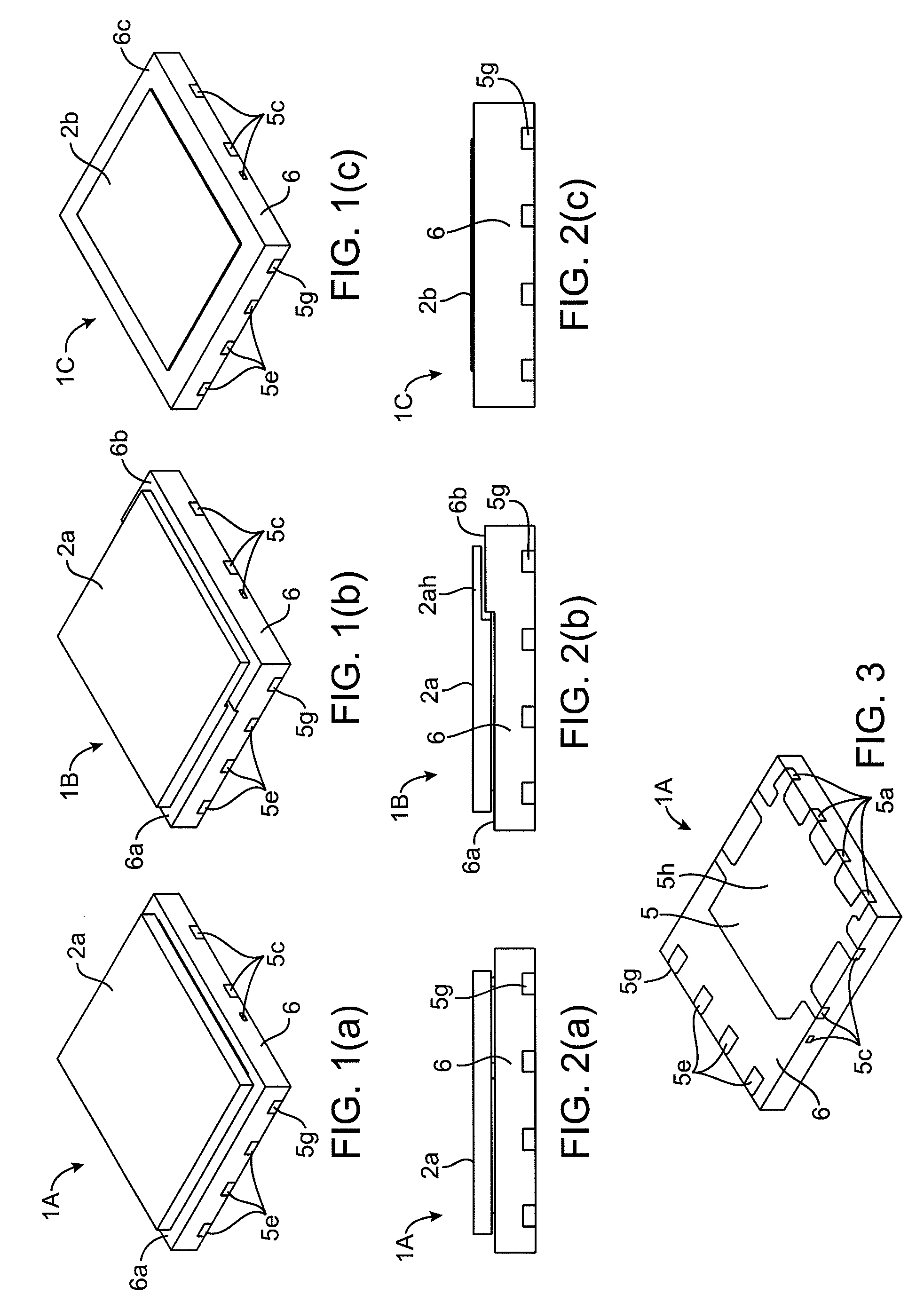
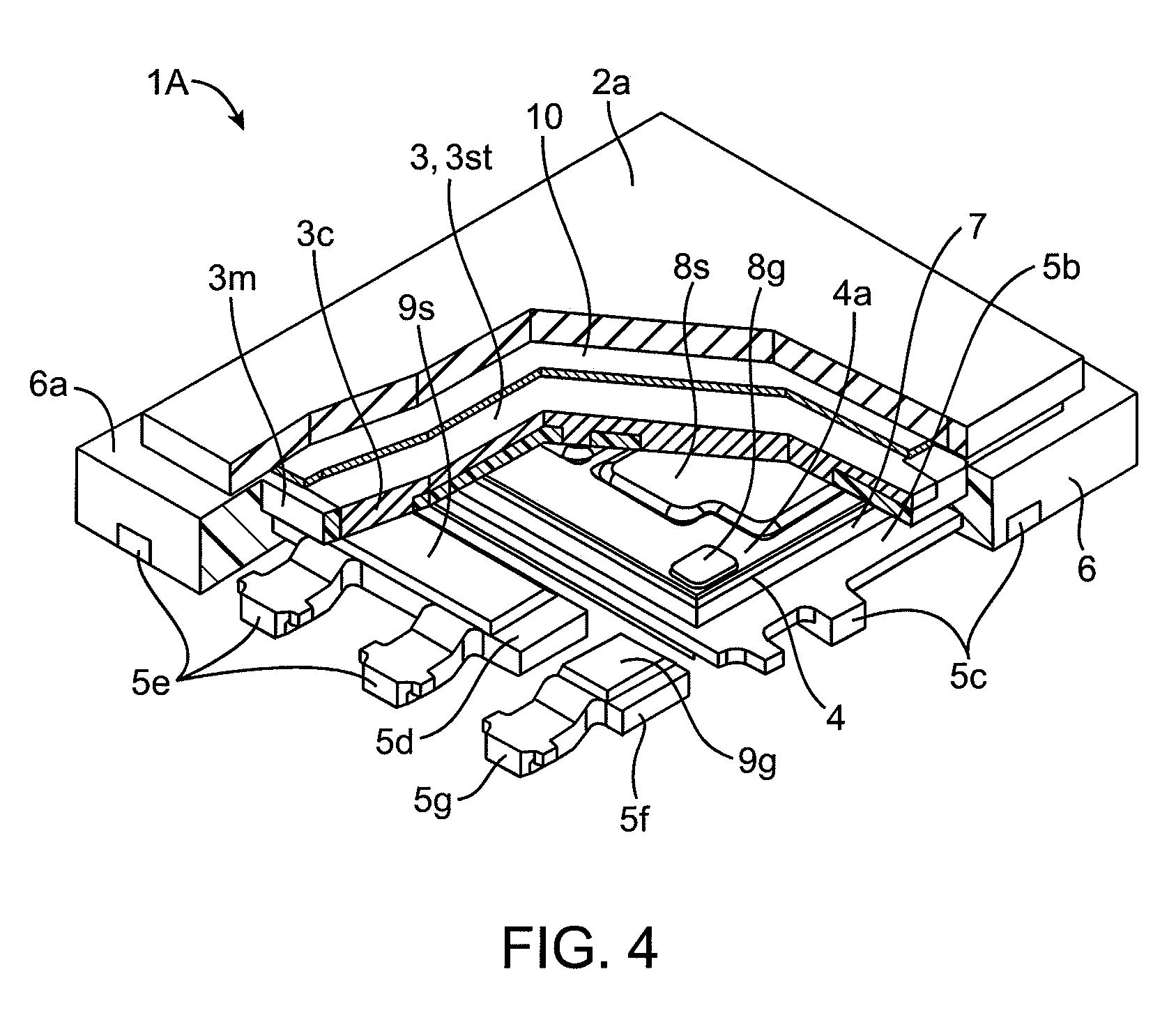
[0043]One embodiment of the invention is directed to a semiconductor die package comprising a semiconductor die and a molded clip structure.

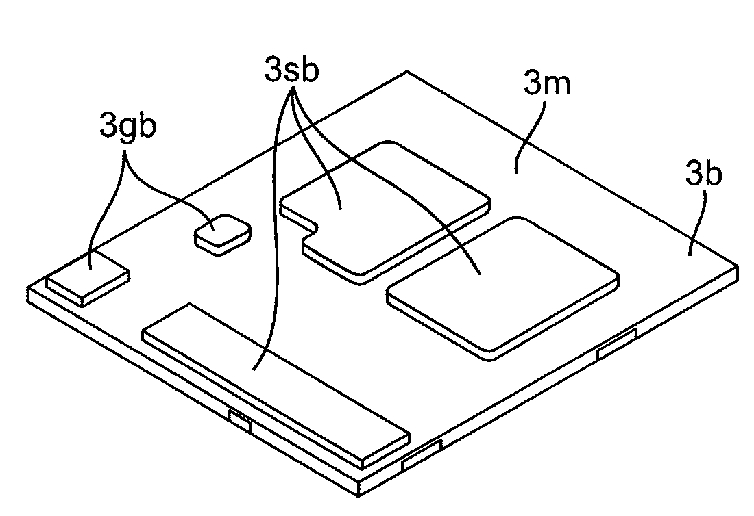
[0044]A semiconductor die in the semiconductor die package may comprise any suitable type of device, including a power MOSFET. While power MOSFETs are described in detail, any suitable vertical power transistor can be used in embodiments of the invention. Vertical power transistors include VDMOS transistors and vertical bipolar transistors. A VDMOS transistor is a MOSFET (an example of which is shown in FIG. 20) that has two or more semiconductor regions formed by diffusion. It has a source region, a drain region, and a gate. The device is vertical in that the source region and the drain region are at opposite surfaces of the semiconductor die. The gate may be a trenched gate structure or a planar gate structure, and is formed at the same surface as the source region. Trenched gate structures are preferred, since trenched gate structures are nar...


PUM


Abstract

A semiconductor die package. The semiconductor die package comprises a semiconductor die and a molded clip structure comprising a clip structure and a first molding material covering at least a portion of the clip structure. The first molding material exposes an outer surface of the clip structure. The clip structure is electrically coupled to the semiconductor die. The semiconductor die package further comprises a leadframe structure comprising a die attach pad and a plurality of leads extending from the die attach pad. The semiconductor die is on the die attach pad of the leadframe structure. A second molding material covers at least a portion of the semiconductor die and the leadframe structure. The semiconductor die package also includes a heat slug and a thermally conductive material coupling the heat slug to the exposed surface of the clip structure.

Description

CROSS-REFERENCES TO RELATED APPLICATIONS[0001]NOT APPLICABLEBACKGROUND[0002]Power semiconductor die packages are known and are used in computers and the like.[0003]Such semiconductor die packages could be improved. For example, power semiconductor die packages generate a significant amount of heat. It would be desirable to improve upon semiconductor die packages so that they can dissipate more heat. Also, conventional semiconductor die packages are molded with a molded material. Having to directly expose a metal clip that is connected to the semiconductor die source contact pad to allow heat dissipation from the top side of the package presents challenges with respect to the metal clip design and the corresponding assembly process (particularly if the standard package dimensions are to be followed). The exposed metal clip stacked on top of the semiconductor die needs to be thick, and this can result in stress to the semiconductor die and the molding material. This can increase the l...

Claims


Application Information

Patent Timeline
Patent Type & Authority Applications(United States)
IPC IPC(8): H01L23/495H01L21/60
CPCH01L23/49524H01L2924/1305H01L24/31H01L24/40H01L2224/83101H01L2224/83191H01L2924/01005H01L2924/01013H01L2924/01027H01L2924/01029H01L2924/01033H01L2924/01047H01L2924/0105H01L2924/01078H01L2924/01082H01L2924/0781H01L2924/13091H01L2924/19041H01L2924/19043H01L23/3107H01L23/4334H01L2224/32245H01L2924/01006H01L2924/014H01L2924/0132H01L23/49562H01L2924/1306H01L2924/10253H01L2224/40247H01L2224/73263H01L2924/00013H01L2224/2929H01L2224/29111H01L2224/29293H01L2924/00014H01L2924/00H01L2924/0665H01L2224/29099H01L2224/29199H01L2224/29299H01L2924/181H01L2224/371H01L2224/37147H01L2224/83801H01L2224/37155H01L2224/84801H01L24/37H01L2224/38H01L24/84H01L24/97H01L2924/00012H01L23/31H01L23/40H01L23/4093H01L2224/40151
Inventor QUINONES, MARIA CLEMENS Y.ESTACIO, MARIA CRISTINA B.
Owner SEMICON COMPONENTS IND LLC
Why Eureka
Try Eureka