Piezoelectric thin film resonant element and circuit component using the same

a thin film resonant element and thin film technology, applied in piezoelectric/electrostrictive/magnetostrictive devices, current collectors, piezoelectric/electrostriction/magnetostriction machines, etc., can solve the problem of aggravated spurious modulation, filter insertion loss, group delay characteristic, etc., to improve resonance characteristics, reduce spurious frequency, and q value higher

Active Publication Date: 2010-06-17
TAIYO YUDEN KK
View PDF16 Cites 38 Cited by
  • Summary
  • Abstract
  • Description
  • Claims
  • Application Information

AI Technical Summary

Benefits of technology

[0032]The present invention has been proposed under the above-described circumstances, and it is therefore an object of the present invention to provide a piezoelectric thin film resonant element which has improved resonance characteristics with a higher Q value, reduced spurious frequencies and reduced energy loss, and a circuit component such as a filter and a branching filter using this piezoelectric thin film resonant element.

Problems solved by technology

As a result, when a plurality of the piezoelectric thin film resonant elements 100 are combined to provide a filter, ripples appear over the pass band of the filter, and in addition it is likely that the filter's insertion loss, group delay characteristic, etc. are decreased.
In these techniques, however, increasing the film thickness tends to improve the spurious modulation but decrease the Q value of the resonance characteristics, while decreasing the film thickness tends to improve the Q value of the resonance characteristics but aggravate the spurious modulation.
In Region (A), however, due to the reflection of the horizontal elastic waves in Region (B), standing wave of the horizontal elastic wave, which can cause spurious modulation, is likely to be generated.
However, at the same time, since leakage of the horizontal elastic waves near the main vibration frequency is increased, the Q value of the resonance characteristics of the piezoelectric thin film resonant element 100 is deteriorated.
Regarding manufacturing a piezoelectric thin film resonant element 100, if the edge of the lower electrode 102a is right-angled, a crack is likely to be formed at the edge portion and the membrane serving forming the resonant portion is likely to be destroyed, whereby reliability is deteriorated.

Method used


Image

  • Piezoelectric thin film resonant element and circuit component using the same
  • Piezoelectric thin film resonant element and circuit component using the same
  • Piezoelectric thin film resonant element and circuit component using the same

Examples


first embodiment

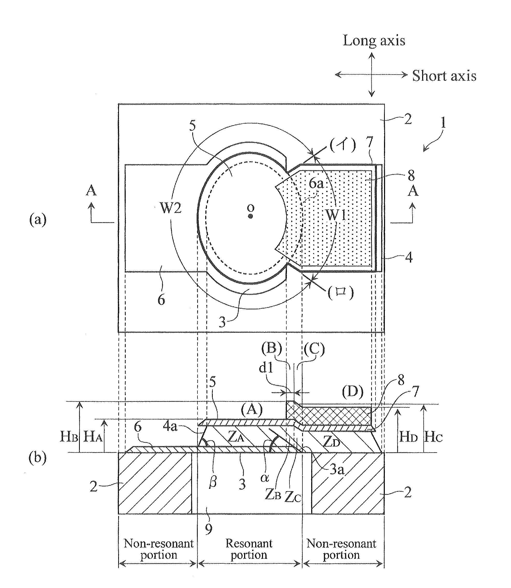
[0074]FIG. 1 illustrates a basic structure of a piezoelectric thin film resonant element according to the present invention. In FIG. 1, (a) is a plan view whereas (b) is a sectional view taken in lines A-A in (a) in the figure. Although the additional film 8 is illustrated slightly inside a terminal electrode 7 in FIG. 1 (A), this is just a drawing technique to clarify that the terminal electrode 7 exists. The actual size of the additional film 8 is substantially the same as that of the terminal electrode 7. Also, an upper electrode 5 and the terminal electrode 7 are drawn in heavy lines for easy visual recognition, and the additional film 8 is distinguished by a dotted pattern. These illustrative features are common in all of the relevant plan views.

[0075]The piezoelectric thin film resonant element 1 illustrated in FIG. 1 is of FBAR (Film Bulk Acoustic Resonator) type. The piezoelectric thin film resonant element 1 includes, as primary constituent members, a substrate 2, a lower e...

second embodiment

[0128]FIG. 14 illustrates a piezoelectric thin film resonant element 1A whereby the additional film 8 is provided only in Region (C) (the region where the inclined portion 3a of the lower electrode 3 is overlapped by the upper electrode 5).

[0129]In the piezoelectric thin film resonant element 1A of the second embodiment, the film thicknesses of Regions (A), (B), (C) and (D) are set to meet the relation HDB=HAC as illustrated in FIG. 14(b), and the acoustic impedances are set to meet the relation ZDB=ZAC. In the second embodiment, the acoustic impedance ZC in Region (C) is greater than the acoustic impedances ZA, ZB and ZD in Regions (A), (B) and (D), and therefore the acoustic impedance mismatch between Regions (A), (B) and Region (D) is great. Thus, lateral elastic waves propagate radially from the center O of the ellipsoidal resonant portion, but the higher-order, symmetric and asymmetric elastic waves of the lateral mode traveling toward the terminal electrode 7 are reflected by...

third embodiment

[0131]FIG. 15 illustrates a piezoelectric thin film resonant element 1B whereby the additional film 8 is provided only in Regions (B) and (C) (the region where the inclined portion 3a of the lower electrode 3 is overlapped by the upper electrode 5 and part of the adjacent inner region).

[0132]In the piezoelectric thin film resonant element 1 of the third embodiment, the film thicknesses of Regions (A), (B), (C) and (D) are set to meet the relation HDACB as illustrated in FIG. 15(b), and the acoustic impedances are set to meet the relation ZDACB. In the third embodiment as well, the acoustic impedances ZB, ZC in Regions (B), (C) are greater than the acoustic impedances ZA, ZD in Regions (A), (D). Therefore, an acoustic impedance mismatch between Region (A) and Region (D) is great, and thus, horizontal elastic waves propagate radially from the center O of the ellipsoidal resonant portion, but the higher-order, symmetric and asymmetric elastic waves of the horizontal mode traveling tow...


PUM


Abstract

A piezoelectric thin film resonant element includes a resonant portion having a laminate structure made up of a lower electrode, an upper electrode and a piezoelectric film arranged between these two electrodes. The lower electrode has an ellipsoidal plan-view shape and an outer circumference formed with an inclined portion inclined at an angle (about 30° for example) lying within a range of 25° through 55°. The upper electrode has an ellipsoidal plan-view shape. An additional film is provided on the upper electrode at a portion corresponding to the inclined portion of the lower electrode.

Description

TECHNICAL FIELD[0001]The present invention relates to a piezoelectric thin film resonant element of FBAR (Film Bulk Acoustic Resonator) type or SMR (Solidly Mounted Resonator) type, while also relating to a circuit component such as a filter and a branching filter using such a piezoelectric thin film resonant element.BACKGROUND ART[0002]As is known, a piezoelectric thin film resonant element has a structure in which a piezoelectric film is sandwiched by electrodes on its upper surface and a lower surface, with a cavity or an acoustic multi-layer film provided below the lower electrode. The piezoelectric thin film resonant element converts an electric signal, applied across the upper and lower electrodes to the piezoelectric film, into a mechanical displacement of the piezoelectric film. In addition, the piezoelectric thin film resonant element responds to a mechanical displacement of a specific frequency, depending on the total thickness of the piezoelectric film, the upper electrod...

Claims


Application Information

Patent Timeline
Patent Type & Authority Applications(United States)
IPC IPC(8): H01L41/047
CPCH03H9/02015H03H9/02086H03H9/02157H03H9/13H03H2003/0428H03H9/174H03H9/175H03H9/568H03H9/132H03H9/02118H03H9/17H03H9/54
Inventor NISHIHARA, TOKIHIROHARA, MOTOAKITANIGUCHI, SHINJIIWAKI, MASAFUMIYOKOYAMA, TSUYOSHIUEDA, MASANORI
Owner TAIYO YUDEN KK
Why Eureka
Try Eureka