Electrostatic discharge circuit and method

a technology of electrostatic discharge and circuit, applied in the direction of emergency protective arrangements for limiting excess voltage/current, emergency protective arrangements for automatic disconnection, instruments, etc., can solve the problems of circuit components in the integrated circuit being damaged, integrated circuit pins being susceptible to electrostatic discharge, and reliability problems during the normal operation of the integrated circui

Active Publication Date: 2010-06-17
ATI TECH INC
View PDF10 Cites 48 Cited by
  • Summary
  • Abstract
  • Description
  • Claims
  • Application Information

AI Technical Summary

Problems solved by technology

Integrated circuit pins are susceptible to receiving electrostatic discharge (ESD) pulses during the assembling process, and in some instances during normal operation.
Improper dissipation of electrostatic discharge pulses can result in the damage to the circuit components in the integrated circuit.
Existing ESD protection circuits can prevent damage from electrostatic discharges but can create reliability problems during the normal operation of the integrated circuit.
For example, a disadvantage of known ESD protection circuits is the possibility of the power to ground shortage during a fast power up condition where the power ramps up at a fast rate when applied to the power nodes of the chip.
In addition, known ESD protection circuits may create reliability problems caused by high frequency noise of voltage supply and ground that may be present on a power supply and ground nodes or rails.
Hence, ESD protection circuits can cause latch up and integrated circuit damage during normal operation of a chip.
However, during a power up event in the case of a fast power up condition or for high frequency power / ground noise, the large time constant for the RC circuit 102 may cause the short of the power rail node 114 to the ground node 116 through shunt structure 112 which may result in a latch up condition and damage to the integrated circuit.
A smaller RC time constant could prevent the shunt structure 112 from seeking current (current spikes) but would make an ESD condition less defensible and not efficient.

Method used


Image

  • Electrostatic discharge circuit and method
  • Electrostatic discharge circuit and method
  • Electrostatic discharge circuit and method

Examples


Embodiment Construction

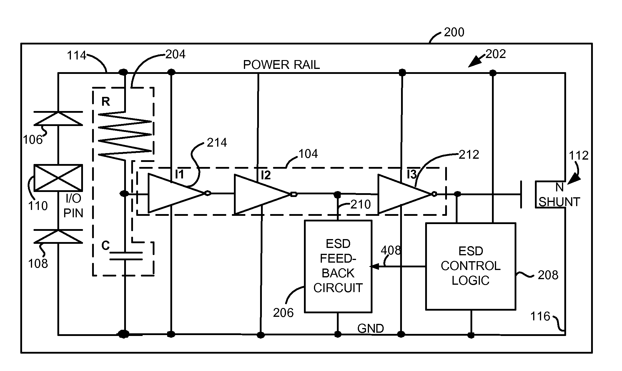
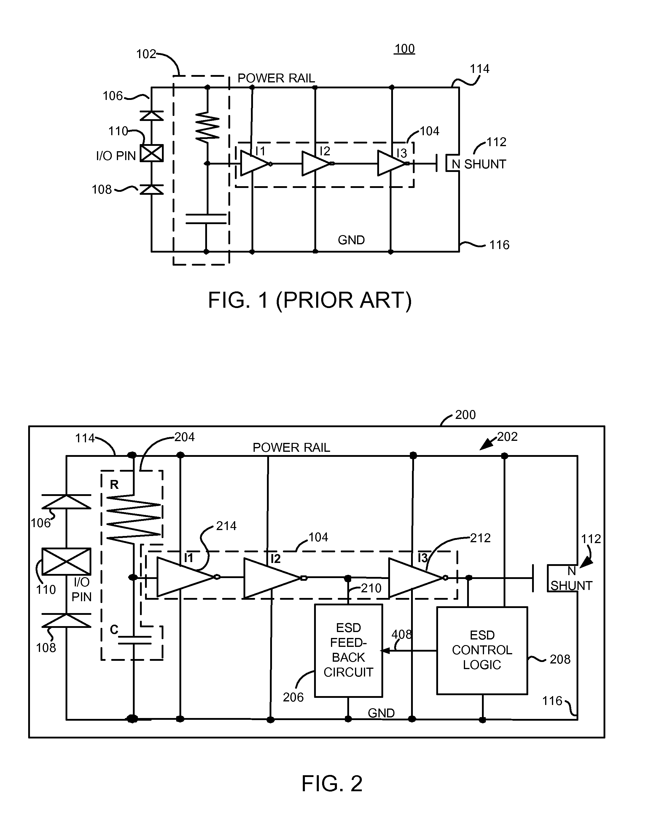
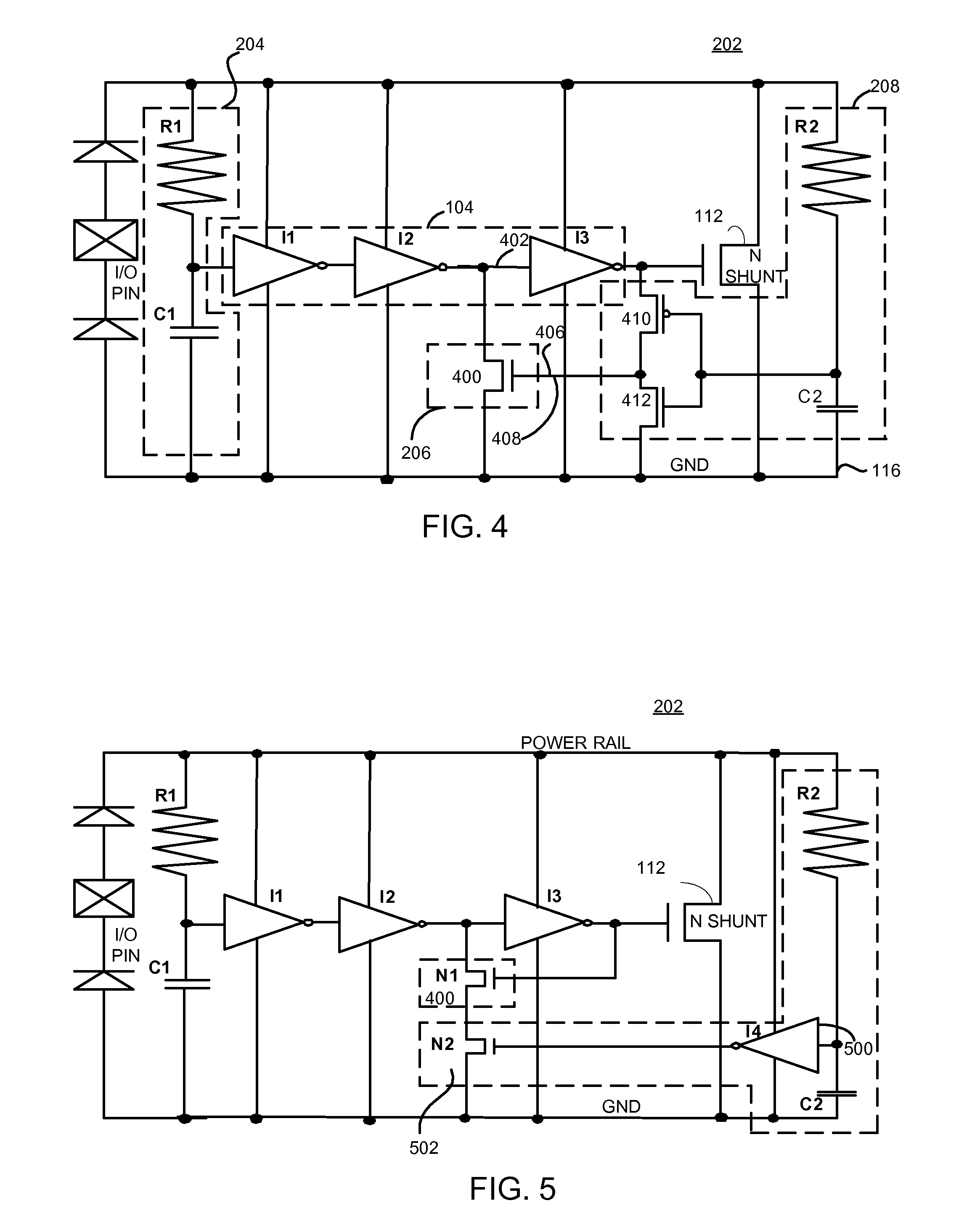
[0013]Briefly, a method and integrated circuit renders a shunt structure non-conductive during a power up event for a period of time or during a noise event and in addition, during an electrostatic discharge event, keeps the shunt structure conductive for a period of time to discharge electrostatic energy through the shunt structure. In one example, a shunt structure, such as a transistor, is interposed between a power node and a ground node. A first circuit is operative during a power up event or noise event, to render the shunt structure non-conductive for a period of time during the power up event or during the noise event (when power is applied). A second circuit is operative, during an electrostatic discharge event, to keep the shunt structure conductive for a period of time to discharge electrostatic energy through the shunt structure. In one example, a plurality of resistor / capacitor blocks (RC blocks) are utilized wherein the RC blocks have different time constants. In addit...


PUM


Abstract

A method and integrated circuit renders a shunt structure non-conductive during a power up event or noise event for and in addition, during an electrostatic discharge event, keeps the shunt structure conductive for a period of time to discharge electrostatic energy through the shunt structure. In one example, a shunt structure, such as a transistor, is interposed between a power node and a ground node. Circuitry is operative during a power up event or noise event, to render the shunt structure non-conductive for a period of time during the power up event or during the noise event (when power is applied). Second circuit is operative, during an electrostatic discharge event, to keep the shunt structure conductive for a period of time to discharge electrostatic energy through the shunt structure. In one example, a plurality of resistor / capacitors (RC) circuits are utilized wherein the RC circuits have different time constants. In addition, an ESD feedback circuit is employed in conjunction with control logic to suitably control the ESD control logic during an ESD event. Circuitry is also used during a power up event to render the shunt structure non-conductive.

Description

FIELD OF THE INVENTION[0001]The disclosure relates to electrostatic discharge circuits and methods and circuits relating to power up protection circuits.BACKGROUND OF THE INVENTION[0002]Integrated circuit pins are susceptible to receiving electrostatic discharge (ESD) pulses during the assembling process, and in some instances during normal operation. Improper dissipation of electrostatic discharge pulses can result in the damage to the circuit components in the integrated circuit. Existing ESD protection circuits can prevent damage from electrostatic discharges but can create reliability problems during the normal operation of the integrated circuit. For example, a disadvantage of known ESD protection circuits is the possibility of the power to ground shortage during a fast power up condition where the power ramps up at a fast rate when applied to the power nodes of the chip. In addition, known ESD protection circuits may create reliability problems caused by high frequency noise o...

Claims


Application Information

Patent Timeline
Patent Type & Authority Applications(United States)
IPC IPC(8): H02H9/04H01L27/06G06F17/50
CPCH02H9/046H01L27/0285
Inventor DRAPKIN, OLEGTEMKINE, GRIGORIBADE, PETER
Owner ATI TECH INC
Why Eureka
Try Eureka