Circuit board device and integrated circuit device

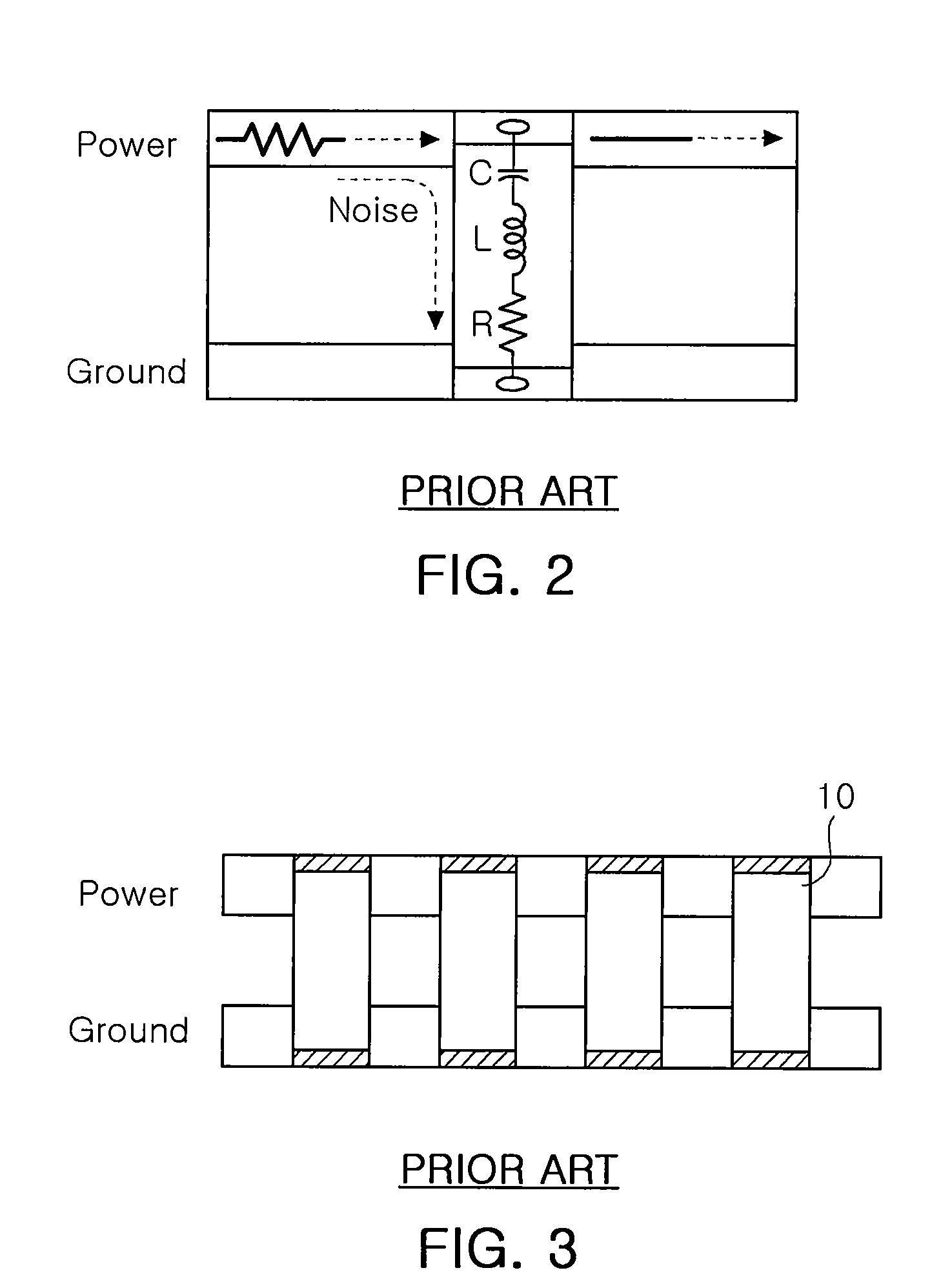
a circuit board and integrated circuit technology, applied in the direction of feed-through capacitors, printed circuit non-printed electric components association, final product manufacture, etc., can solve the problems of increasing the impedance of the capacitor, degrading the function of the bypass capacitor, and complicated power circuit configuration, so as to simplify the power circuit configuration and remove the effect of high frequency nois

Active Publication Date: 2010-06-17
SAMSUNG ELECTRO MECHANICS CO LTD
View PDF2 Cites 70 Cited by
  • Summary
  • Abstract
  • Description
  • Claims
  • Application Information

AI Technical Summary

Benefits of technology

[0011]An aspect of the present invention provides a circuit board device including a multilayer chip capacitor (MLCC) capable of effectively removing high frequency noise while retaining high rated-current characteristics and simplifying a power circuit configuration.
[0014]The vertical MLCC may further include a fourth outer electrode having the same polarity as that of the third outer electrode and formed between the first and second outer electrodes on an upper face of the capacitor body. In this case, the MLCC may be vertically symmetrical in its internal and external structures, and accordingly, the MLCC can be mounted regardless of a mounting direction, providing convenience.

Problems solved by technology

In this case, however, the MLCC has both equivalent series resistance (ESR) and equivalent series inductance (ESL) components in addition to a capacitance component, and such ESR and ESL components degrade the function of the bypass capacitor.
In particular, the ESL components increase the impedance of the capacitor at high frequencies to degrade high frequency noise removing characteristics.
However in this method, the increase in the number of capacitors makes the power circuit configuration complicated.

Method used


Image

  • Circuit board device and integrated circuit device
  • Circuit board device and integrated circuit device
  • Circuit board device and integrated circuit device

Examples


Embodiment Construction

[0033]Exemplary embodiments of the present invention will now be described in detail with reference to the accompanying drawings. The invention may however be embodied in many different forms and should not be construed as limited to the embodiments set forth herein. Rather, these embodiments are provided so that this disclosure will be thorough and complete, and will fully convey the scope of the invention to those skilled in the art. In the drawings, the shapes and dimensions may be exaggerated for clarity, and the same reference numerals will be used throughout to designate the same or like components.

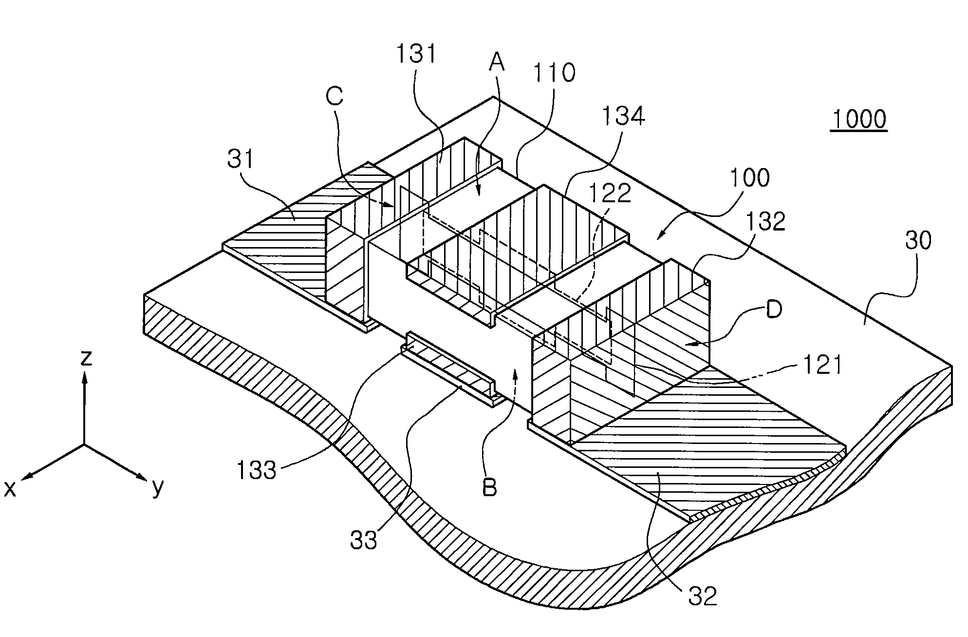
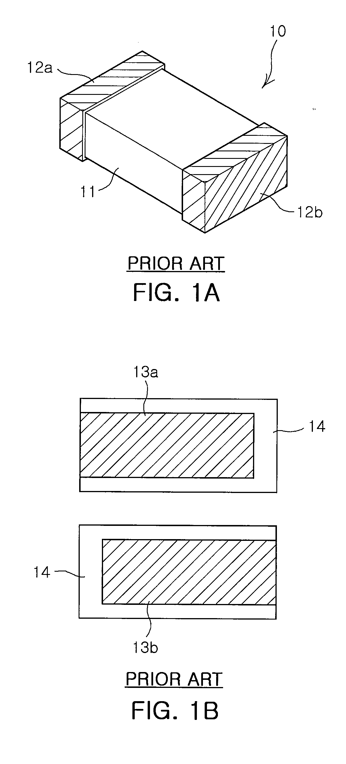
[0034]FIG. 4 is a perspective view illustrating a circuit board device according to an embodiment of the present invention, and FIG. 5 is a vertical sectional view of FIG. 4. With reference to FIGS. 4 and 5, a circuit board device 1000 according to an embodiment of the present invention has a structure in which a three-terminal vertical multilayer chip capacitor (MLCC) 100 is mounte...


PUM

PropertyMeasurementUnit
areaaaaaaaaaaa
polarityaaaaaaaaaa
polaritiesaaaaaaaaaa

Abstract

A circuit board device includes a circuit board comprising a mounting area, and first and second power lines and a ground pad formed on the mounting area, and a vertical multilayer chip capacitor (MLCC) comprising a capacitor body, a plurality of first and second polarity inner electrodes, first and second outer electrodes, and a third outer electrode, wherein the first and second power lines are separately disposed on the mounting area, connected to the first and second outer electrodes, and electrically connected to each other only by the vertical MLCC, and the ground pad is disposed between the first and second power lines and connected to the third outer electrode.

Description

CROSS-REFERENCE TO RELATED APPLICATIONS[0001]This application claims the priority of Korean Patent Application No. 2008-0126728 filed on Dec. 12, 2008, in the Korean Intellectual Property Office, the disclosure of which is incorporated herein by reference.BACKGROUND OF THE INVENTION[0002]1. Field of the Invention[0003]The present invention relates to a circuit board device with a multilayer chip capacitor mounted thereon and an integrated circuit device, and more particularly, to a circuit board device and an integrated circuit device capable of effectively removing high frequency noise while retaining high rated-current characteristics and simplifying a power circuit configuration.[0004]2. Description of the Related Art[0005]A multilayer chip capacitor (MLCC) is favorably used as a bypass capacitor disposed within a power circuit of LSI (Large Scale Integration). To serve as the bypass capacitor, the MLCC needs to effectively remove high frequency noise. Such a need is increasing i...

Claims


Application Information

Patent Timeline
Patent Type & Authority Applications(United States)
IPC IPC(8): H05K1/18
CPCH01G2/065H01G4/35H05K1/0231H05K2201/10969H05K2201/09481H05K2201/10636H05K2201/09318Y02P70/50H01G4/12H01G4/228H05K1/18
Inventor LEE, BYOUNG HWAWI, SUNG KWONCHO, HONG YEONPARK, DONG SEOKPARK, SANG SOOPARK, MIN CHEOL
Owner SAMSUNG ELECTRO MECHANICS CO LTD
Why Eureka
Try Eureka