Linearized optical digital-to-analog modulator

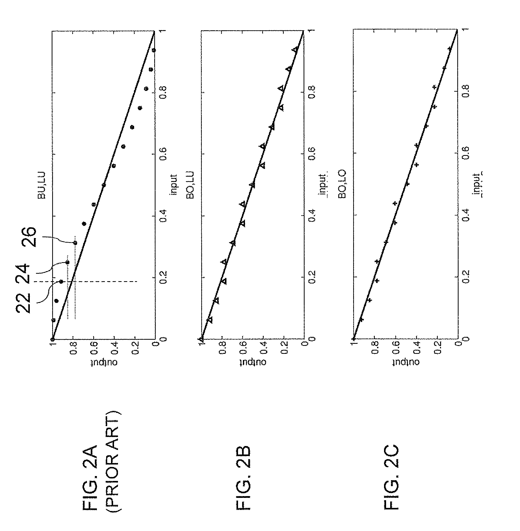
a linearized optical and analog modulator technology, applied in the field of optical modulators, can solve the problems of severe dynamic range limitation, non-linear response of the modulator, and subsequently the attainable resolution

Active Publication Date: 2010-06-24
RAMOT AT TEL AVIV UNIV LTD
View PDF5 Cites 45 Cited by
  • Summary
  • Abstract
  • Description
  • Claims
  • Application Information

AI Technical Summary

Problems solved by technology

For analog applications, however, a serious problem is encountered due to the inherent non-linear response of the modulator.
In that device, the electrodes' sectioning length followed a conventional power-of-two digital sequence, which did not solve the non-linearity problem, and thus suffered from severe limitation in the dynamic range, and subsequently the attainable resolution.
More recently, much more complex devices have been presented to cope with these problems: Yacoubian et al.

Method used


Image

  • Linearized optical digital-to-analog modulator
  • Linearized optical digital-to-analog modulator
  • Linearized optical digital-to-analog modulator

Examples


example i

Mach-Zehnder Modulator

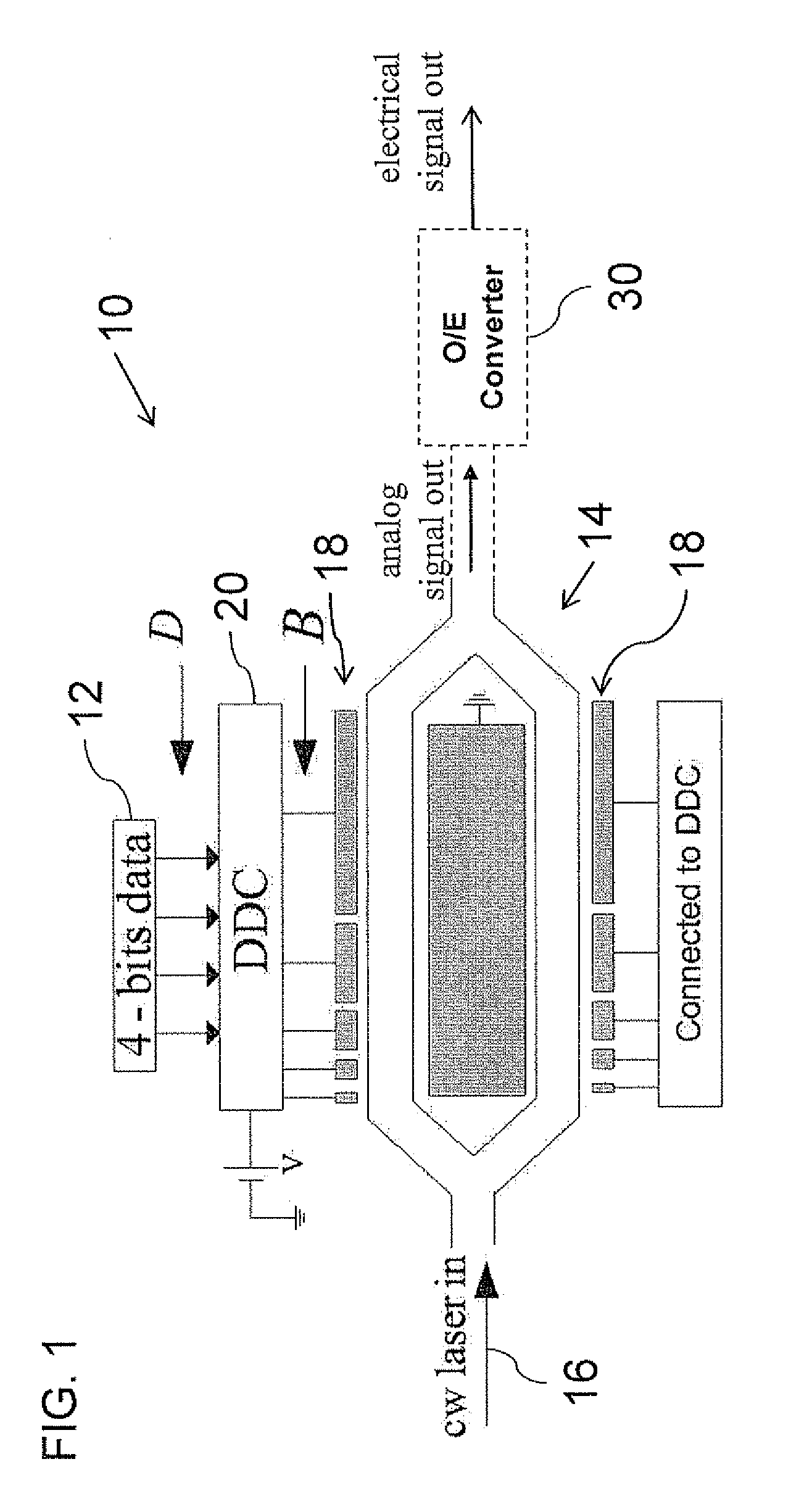
[0072]By way of example, there will now be presented a theoretical treatment of one particularly preferred example of modulator device 10 implemented using a Mach-Zehnder modulator, also referred to as a Mach-Zehnder Interferometer or “MZI”. This theoretical treatment is presented to facilitate an understanding of the present invention and as a suggested technique for calculating certain parameters. However, it should be noted that the invention as described above has been found to be effective, independent of the accuracy or otherwise of this theoretical treatment.

[0073]The Mach-Zehnder modulator is an active integrated waveguide device consisting of a higher index guide region that splits into two paths which are combined again after a certain distance. Each of these paths is referred to as a leg or branch. When used as a switch, the MZI may be turned “off” by raising or lowering the index of refraction in one of the legs. This is achieved by employing the el...

example ii

Electro-Absorption Modulator

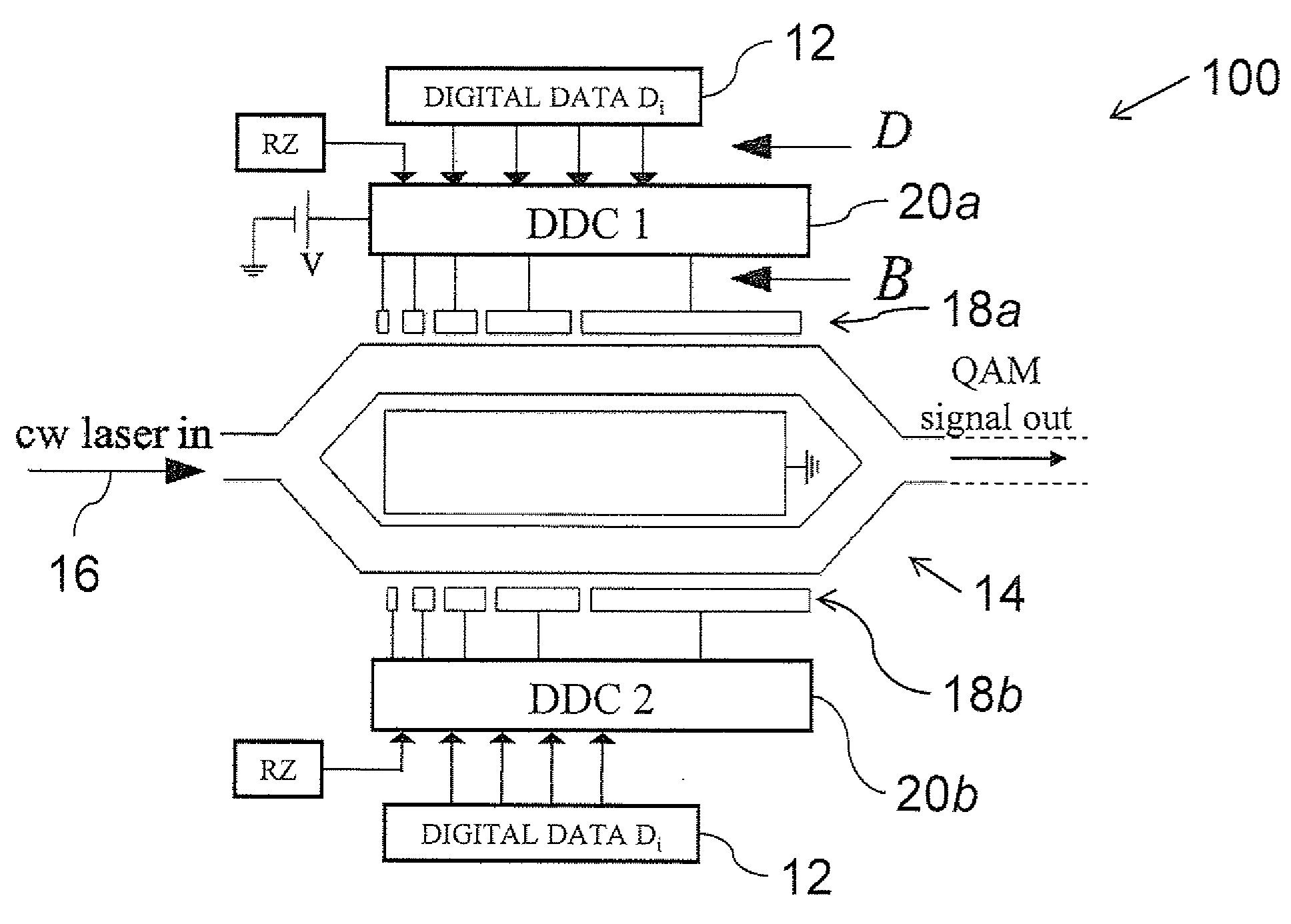
[0086]As mentioned earlier, the present invention is not limited to implementations based on Mach-Zehnder modulators, and can be implemented using any device which modulates light intensity as a function of applied voltage. By way of one additional non-limiting implementation, FIG. 8 shows an analogous implementation of the present invention using an electro-absorption modulator.

[0087]An electro-absorption modulator (EAM) is a semiconductor device which allows control of the intensity of a laser beam via an electric voltage. Its operational principle is typically based on the Franz-Keldysh effect, i.e., a change of the absorption spectrum caused by an applied electric field, which usually does not involve the excitation of carriers by the electric field.

[0088]By realizing N or more electrodes we can use the EAM as a high speed electro-optical Digital-to-Analog converter, in a similar fashion as we used the MZI. As in modulator device 10 described above, t...

example iii

Modulated Light Generation Device

[0090]The present invention is applicable also to other devices where digital information carried by voltage or current is translated into analog optical signals in the form of optical power. This includes also light generation devices like Light Emitting Diodes (LED) or semiconductor lasers. By way of illustration, FIG. 9 shows a semiconductor laser implementation of the present invention.

[0091]Specifically, FIG. 9 shows a semiconductor laser DAC device, generally designated 40, constructed and operative according to the teachings of the present invention. The actuating electrode, typically implemented as a single contiguous electrode, is here subdivided into a threshold electrode 42 and M actuating electrodes 18. The threshold electrode 42 is typically needed to reach a minimum activation current below which no significant output is generated. Actuating electrodes 18 are actuated as a function of the data bits of a digital input 12, in this case a ...


PUM

PropertyMeasurementUnit
actuating voltageaaaaaaaaaa
phaseaaaaaaaaaa
actuating voltagesaaaaaaaaaa

Abstract

A modulator device for converting digital data into modulation of an optical signal includes an electronic input for receiving an input data word of N bits and an electrically controllable modulator for modulating the intensity of an optical signal, the modulator including M actuating electrodes where M≧N. An electrode actuating device, most preferably a digital-to-digital converter, operates actuating electrodes so that at least one electrode is actuated as a function of values of more than one bit of the input data word. According to an alternative, or supplementary, aspect of the invention, the set of electrodes includes at least one electrode having an effective area which is not interrelated to others of the set by factors of two. In one preferred implementation, a Mach-Zehnder modulator also provides phase modulation to give QAM functionality. Another implementation employs a semiconductor laser.

Description

[0001]This is a continuation in part of PCT Patent Application No. PCT / IL08 / 000,805 filed Jun. 12, 2008, published as WO 2008 / 152642, which benefits from the filing date of Provisional Application No. 60 / 943,559 filed Jun. 13, 2007.FIELD AND BACKGROUND OF THE INVENTION[0002]The present invention relates to optical modulators and, in particular, it concerns a linearized optical digital-to-analog modulator.[0003]There is a tangible need for high-performance and large bandwidth digital to analog signal conversion. Furthermore, as the RF and digital domains converge, entirely new solutions will be needed to enable multi-GHz mixed-signal systems. Probably the most prominent area to benefit is the wireless communication industry. The ever increasing thirst for bandwidth will require data converters to deliver greatly increased performance. For example, analog signals are transmitted in cable television (CATV) via optical fibers and the demand for increasing bandwidth is driving technology...

Claims


Application Information

Patent Timeline
Patent Type & Authority Applications(United States)
IPC IPC(8): G02F1/01H03M7/00
CPCG02F1/0121G02F1/015G02F7/00G02F2001/212G02F1/225H04B10/5055H04B10/2575H04B10/516G02F2203/19H04B10/505H03M1/70H04B10/541G02F1/212H04B10/25891H04B10/556H03M1/002
Inventor EHRLICHMAN, YOSSEFAMRANI, OFERRUSCHIN, SHLOMO
Owner RAMOT AT TEL AVIV UNIV LTD
Why Eureka
Try Eureka