Magnetoresistive memory cell using floating body effect, memory device having the same, and method of operating the memory device

a floating body effect and magnetic memory technology, applied in the field of magnetic random access memory (mram), can solve the problems of flash memory having non-volatile characteristics, data loss, power loss increase, etc., and achieve the effect of improving the current driving capability of a select transistor

Active Publication Date: 2010-06-24
SK HYNIX INC
View PDF1 Cites 81 Cited by
  • Summary
  • Abstract
  • Description
  • Claims
  • Application Information

AI Technical Summary

Benefits of technology

[0015]Accordingly, exemplary embodiments of the present invention provide a magnetoresistive memory cell, which can improve the current driving capability of a select transistor required for a high-integration

Problems solved by technology

Dynamic Random Access Memory (DRAM), which is a representative memory device that is currently widely used, is advantageous in that high-speed operation and high integration are possible, but is disadvantageous in that, since DRAM is volatile memory, data is lost when power is turned off, and in that, since data must be continuously rewritten through a data refresh operation even during the operation of the DRAM, power loss increases.
On the other hand, flash memory having characteristics of non-volatility and high integration is disadvantageous in that the operating speed is low.
However, it is difficult to drive current sufficiently high to write information in the MTJ device by using a micro-transistor required for the implementation of high-integration memory.
In the region P of saturated current flow, it is difficult to obtain high current due to the saturation of current even if a drain-source voltage is increased.
Therefore, when a MOS transistor is formed on a bulk silicon substrate as in the case of the prior art, the size of

Method used


Image

  • Magnetoresistive memory cell using floating body effect, memory device having the same, and method of operating the memory device
  • Magnetoresistive memory cell using floating body effect, memory device having the same, and method of operating the memory device
  • Magnetoresistive memory cell using floating body effect, memory device having the same, and method of operating the memory device

Examples


Embodiment Construction

[0029]Hereinafter, embodiments of the present invention will be described in detail with reference to the attached drawings. Reference now should be made to the drawings, in which the same reference numerals are used throughout the different drawings to designate the same or similar components. In the following description of the present invention, detailed descriptions may be omitted to the extent that providing the detailed descriptions of related well-known constructions or functions may make the crux of the present invention unclear.

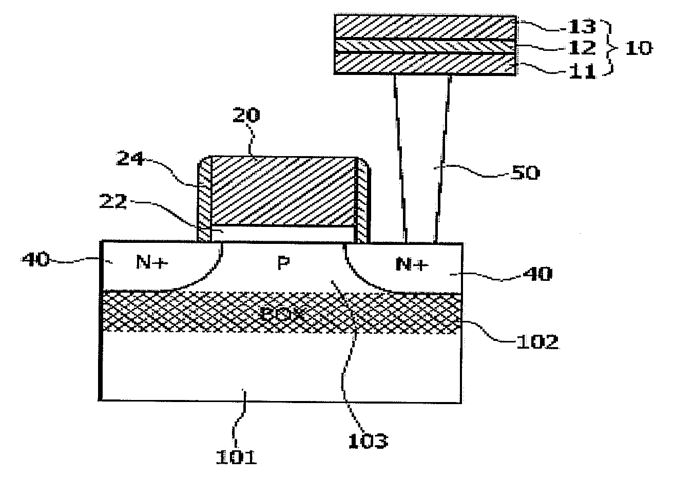
[0030][Memory Cell Configuration]

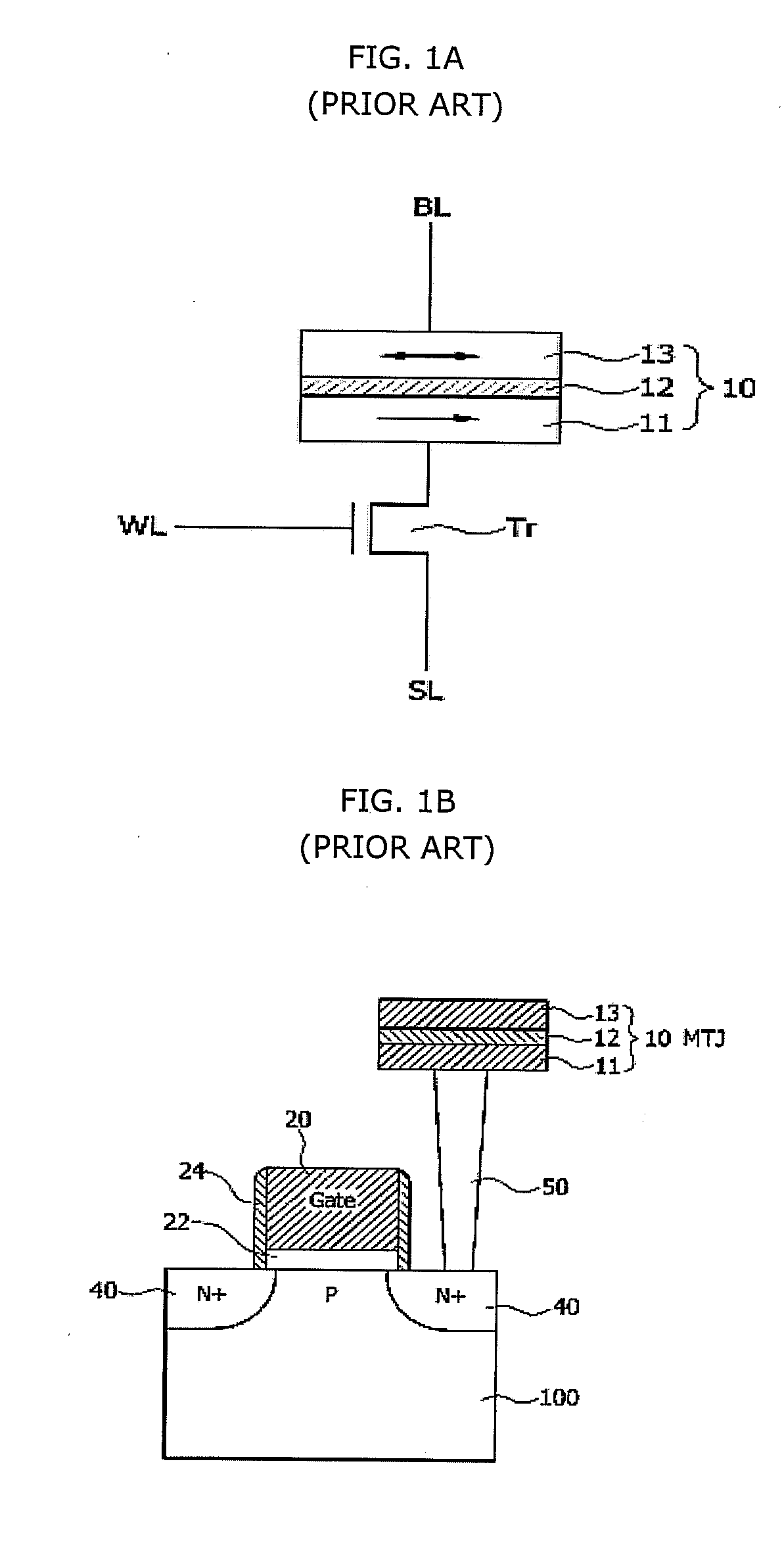
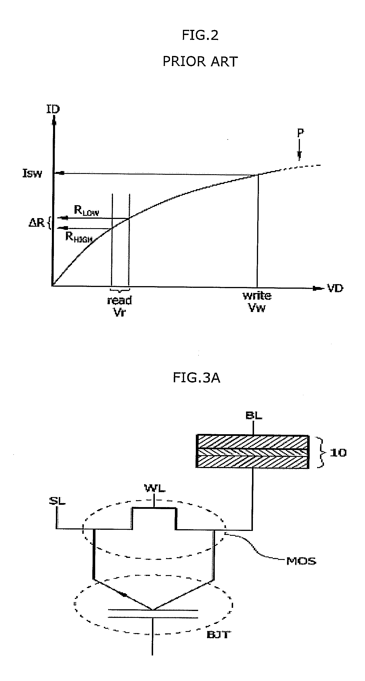
[0031]FIGS. 3A and 3B are an equivalent circuit diagram and a sectional view, respectively, of a magnetoresistive memory cell according to an embodiment of the present invention. Referring to FIGS. 3A and 3B, a select transistor functioning as a switching device has a structure in which a MOS transistor Tr and a Bipolar Junction Transistor (BJT) are coupled to each other. The select transistor having this structure ca...


PUM


Abstract

A magnetoresistive memory cell includes an MTJ device and a select transistor. The select transistor includes a first conduction-type semiconductor layer, a gate electrode formed by disposing a gate insulating layer on top of the semiconductor layer, and first and second diffusion regions formed in the semiconductor layer to be spaced apart from each other and to have a second conduction type. A part of the semiconductor layer between the first and second diffusion regions is formed as an electrically floating body region. By using a high-performance select transistor with a floating body effect, high integration of a magnetoresistive memory device may be achieved.

Description

CROSS-REFERENCE TO RELATED APPLICATIONS[0001]The present invention claims priority of Korean patent application number 10-2008-0132652, filed on Dec. 23, 2008, the disclosure of which is incorporated by reference herein in its entirety.BACKGROUND OF THE INVENTION[0002]1. Field of the Invention[0003]The present invention relates, in general, to Magnetic Random Access Memory (MRAM), and, more particularly, to a non-volatile memory device which uses magnetoresistance variation.[0004]2. Description of the Related Art[0005]Dynamic Random Access Memory (DRAM), which is a representative memory device that is currently widely used, is advantageous in that high-speed operation and high integration are possible, but is disadvantageous in that, since DRAM is volatile memory, data is lost when power is turned off, and in that, since data must be continuously rewritten through a data refresh operation even during the operation of the DRAM, power loss increases. On the other hand, flash memory ha...

Claims


Application Information

Patent Timeline
IPC IPC(8): G11C11/00H01L29/82G11C11/14H01L29/76
CPCG11C11/16H01L29/7841H01L27/228H01L27/1203G11C13/003G11C2213/79G11C11/1659G11C11/1673G11C11/1675G11C11/1693H10B61/22G11C11/15G11C11/21G11C11/34
Inventor CHUNG, SUNG WOONG
Owner SK HYNIX INC
Why Eureka
Try Eureka