Embedded Memory Repair

a technology of embedded memory and repair technique, applied in the field of techniques, can solve the problems of memory cells being prone to manufacturing failures, ic with equal areas of embedded memory and logic, and soc technologies, etc., and achieve the effect of efficient repair of embedded memory

Inactive Publication Date: 2010-06-24
BROADCOM INT PTE LTD
View PDF24 Cites 27 Cited by
  • Summary
  • Abstract
  • Description
  • Claims
  • Application Information

AI Technical Summary

Benefits of technology

[0007]The present invention, in illustrative embodiments thereof, comprises techniques for efficiently repairing embedded memory in an IC. A pair of state machines is employed to automatically program fuse registers based on memory built-in self-test (MBIST) results associated with the embedded memory and to download the information programmed into the fuse registers for performing a rerouting of memory addresses corresponding to failed memory instances in the embedded memory.

Problems solved by technology

Densely packing the memory cells makes them prone to manufacturing failures.
An IC with equal areas of embedded memory and logic (as in the case of SoC technologies) is likely to fail due to manufacturing defects in memory twice as often as it will fail due to defects in logic.
However, the inclusion of redundant memory cells in an IC can undesirably increase the size of the IC.
Thus, there is a trade-off between increased yield on the one hand and increased chip size and complexity on the other hand.

Method used


Image

  • Embedded Memory Repair
  • Embedded Memory Repair
  • Embedded Memory Repair

Examples


Embodiment Construction

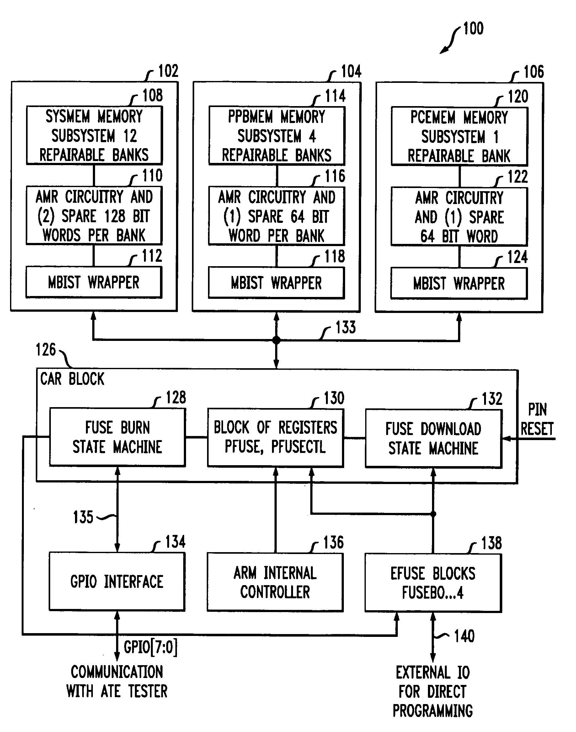
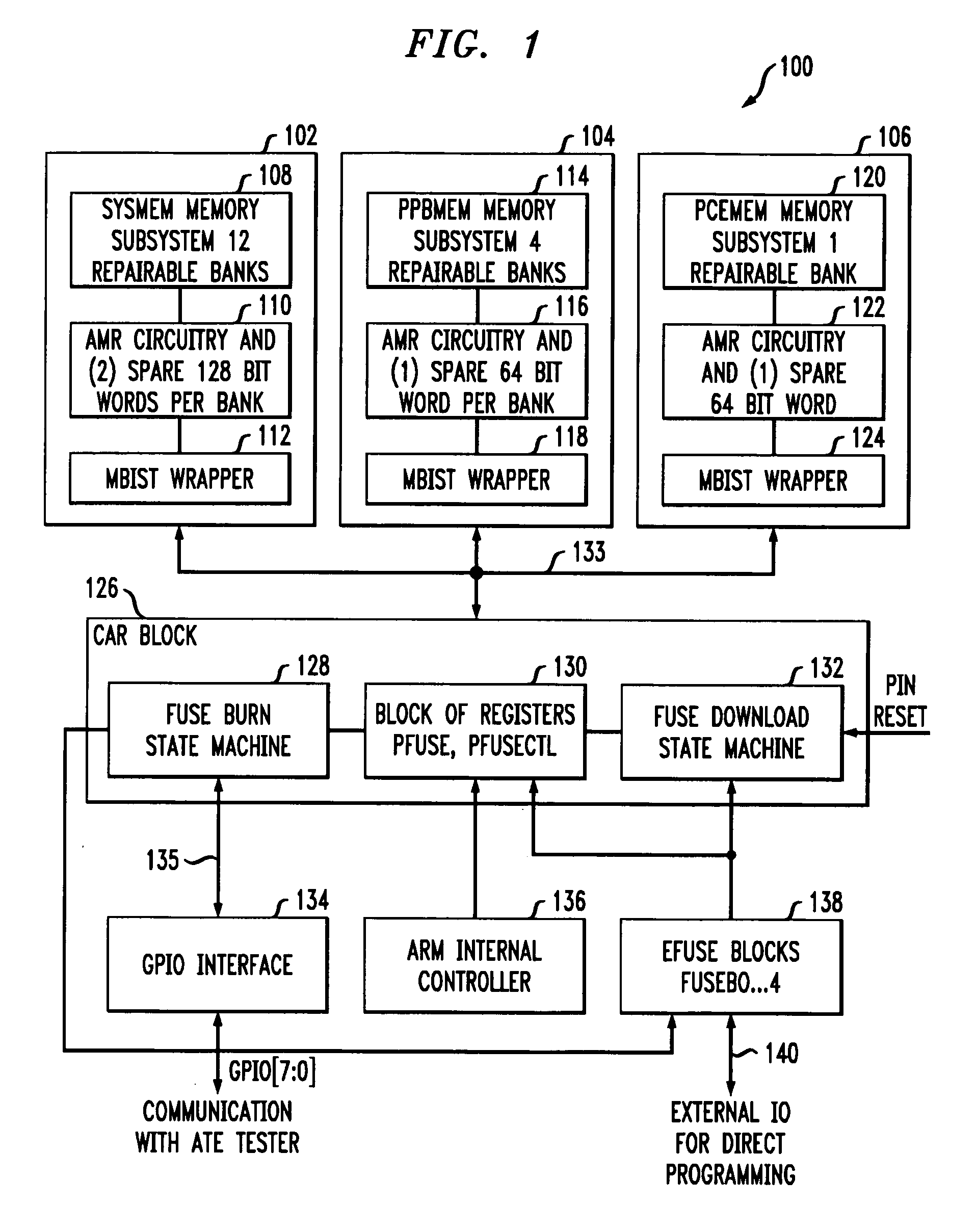
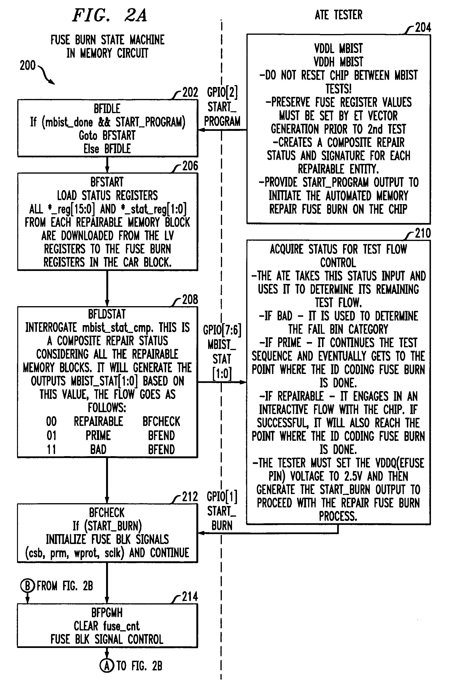
[0019]The present invention will be described herein in the context of exemplary methods and apparatus for repairing embedded memory in an IC device so as to increase a manufacturing yield of functioning devices. It is to be understood, however, that the techniques of the present invention are not limited to the methods and apparatus shown and described herein.

[0020]A “device” as the term is used herein may comprise, by way of example only and without limitation, elements such as those commonly associated with an application-specific integrated circuit (ASIC), single inline memory module (SIMM), dual inline memory module (DIMM), content-addressable memory (CAM), central processing unit (CPU), digital signal processor (DSP), or any other type of data processing or storage device, as well as portions and / or combinations of such elements having embedded memory. A “memory” as the term is used herein is intended to refer broadly to any element that can be employed to at least temporarily...


PUM


Abstract

A memory repair circuit for repairing one or more failures in an embedded memory includes at least one fuse register and state machine circuitry coupled to the fuse register. The state machine circuitry implements a first state machine operative: (i) to receive status information regarding the one or more failures in the embedded memory; (ii) to determine whether the memory is repairable based on the status information; (iii) when the memory is deemed repairable, to store an address corresponding to a failed memory cell of the memory; (iv) to burn the address corresponding to the failed memory cell into the fuse register using a voltage source supplied to the memory repair circuit; and (v) to verify that the address corresponding to the failed memory cell was burned into the fuse register. The state machine circuitry further implements a second state machine operative: (i) to download information stored in the at least one fuse register into at least one repair register associated with the embedded memory; and (ii) when an address is received in the circuit corresponding to a failed memory instance in the embedded memory, to reroute access to the failed memory instance to the at least one repair register.

Description

FIELD OF THE INVENTION[0001]The present invention relates generally to techniques for increasing yield in semiconductor devices, and more particularly relates to techniques for repairing embedded memory in an integrated circuit (IC).BACKGROUND OF THE INVENTION[0002]Semiconductor memory devices, including, for example, read-only memory (ROM), random access memory (RAM), etc., typically include an array of memory cells arranged in rows and columns. Each of the memory cells stores information, often referred to as a bit, in one of two logic states, namely, a logic high state (a logic “1”) and a logic low state (a logic “0”). To access the information stored in a given memory cell, a unique address is utilized. The memory address for each memory cell typically incorporates the particular row and column location of the memory cell in the memory array.[0003]With process technologies pushing well into deep-submicron geometries, IC designers can integrate significant densities of memory and...

Claims


Application Information

Patent Timeline
Patent Type & Authority Applications(United States)
IPC IPC(8): G11C29/00G11C17/18
CPCG11C29/027G11C29/44G11C2029/0401G11C29/72G11C29/4401G11C8/04G11C29/04
Inventor FISCHER, FREDERICK HARRISONMARTIN, RICHARD P.
Owner BROADCOM INT PTE LTD
Why Eureka
Try Eureka