Method of manufacturing through-silicon-via and through-silicon-via structure

Inactive Publication Date: 2010-07-01
IND TECH RES INST
View PDF5 Cites 106 Cited by
  • Summary
  • Abstract
  • Description
  • Claims
  • Application Information

AI Technical Summary

Benefits of technology

[0007]The present invention provides a method for manufacturing a through-silicon-via. In the method, a first annular trench is formed in a silicon substrate, and a first conductive layer, a capacitor dielectric layer, and a second conductive layer are then formed in the first annular trench, sequentially. Next, an opening is formed in the silicon substrate surrounded by the first annular trench. An insulating layer is then formed on an inner surface of the opening, and a conductive material is filled into the opening. Thereafter, a planarization process is performed on a back of the silicon substrate for removing a portion of the silicon substrate, which simultaneously removes the insulating layer from a bottom of the opening to form a conductive through-via and removes the first conductive layer and the capacitor dielectric layer from a bottom of the first annular trench. Then, the silicon substrate, the first conductive layer, and the capacitor dielectric layer between the insulating layer and the second conductive layer are remov

Problems solved by technology

However, the annular TSV structures only p

Method used


Image

  • Method of manufacturing through-silicon-via and through-silicon-via structure
  • Method of manufacturing through-silicon-via and through-silicon-via structure
  • Method of manufacturing through-silicon-via and through-silicon-via structure

Examples


Embodiment Construction

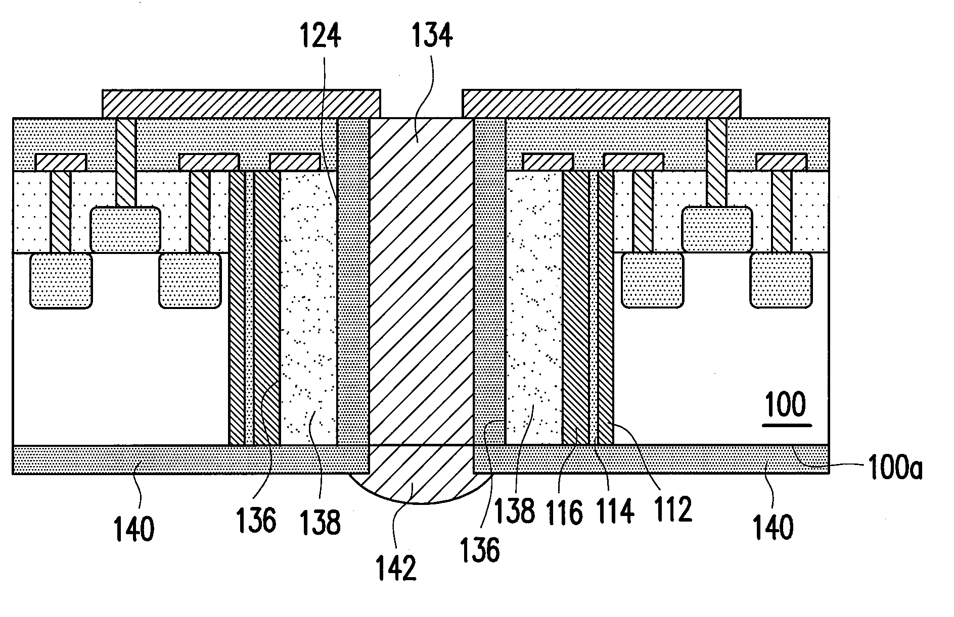
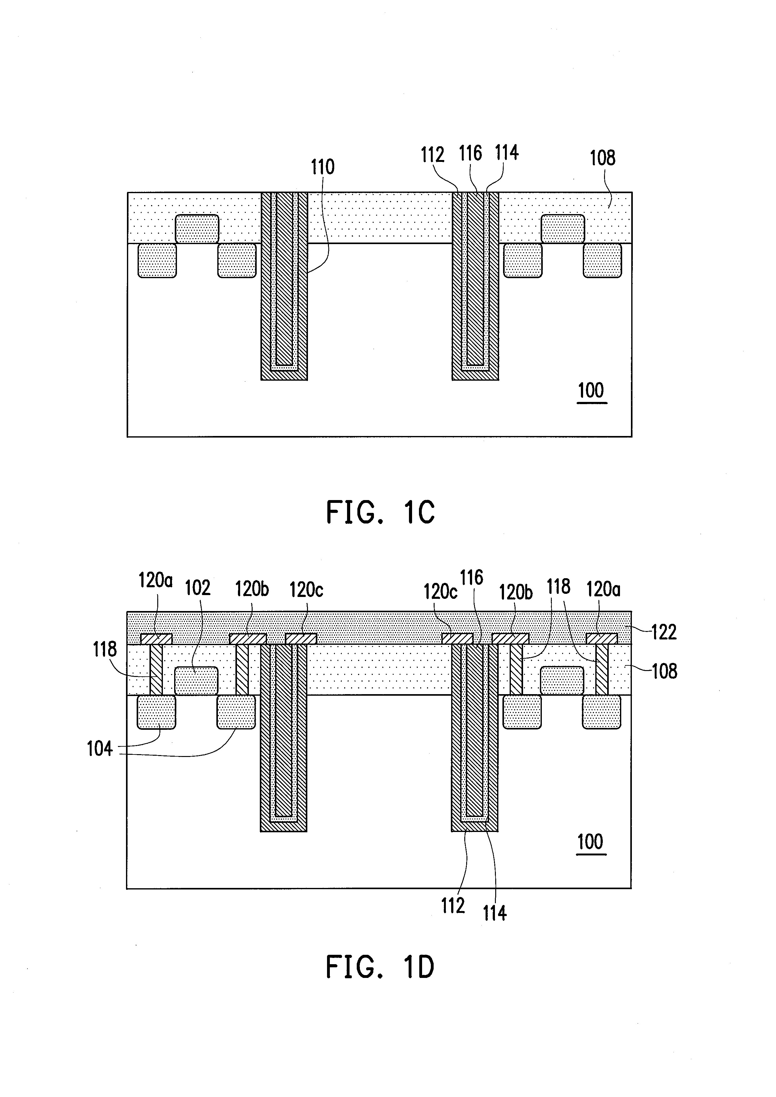
[0014]FIGS. 1A-1J are schematic cross-sectional views illustrating a process flow for manufacturing a through-silicon-via according to one embodiment of the present invention.

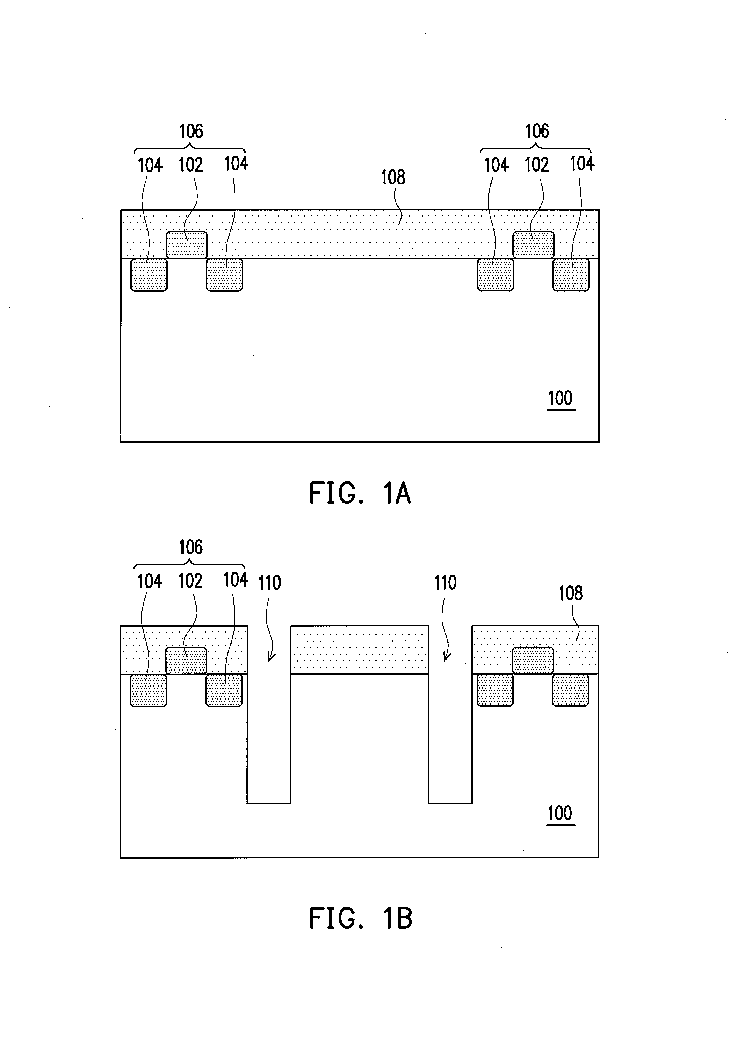
[0015]Referring to FIG. 1A, a fabricating method described in this embodiment may be integrated with the current IC fabricating process. Hence, a front-end transistor fabricating process may be carried out before manufacturing the through-silicon-via. The said front-end transistor fabricating process is, for example, to form a transistor 106 each constituted of a gate 102 and two source / drain 104 on a silicon substrate 100 and then cover the silicon substrate 100 with an inner dielectric (ILD) layer 108. The position and number of the transistor 106 in FIG. 1A may be varied to meet the actual requirements, and the present invention is not limited to the above.

[0016]Then, referring to FIG. 1B, a dry etching process is adopted to form a first annular trench 110 in the silicon substrate 100, wherein a dry etching ...


PUM


Abstract

A method of manufacturing through-silicon-via (TSV) and a TSV structure are provided. The TSV structure includes a silicon substrate, an annular capacitor, a conductive through-via, a layer of low-k material, and a bump. The annular capacitor is within the silicon substrate and constituted of a first conductive layer, a capacitor dielectric layer, and a second conductive layer from the inside to the outside. The conductive through-via is disposed in the silicon substrate surrounded by the annular capacitor, and the layer of low-k material is between the annular capacitor and the conductive through-via. The bump is in touch with the conductive through-via for bonding other chip.

Description

CROSS-REFERENCE TO RELATED APPLICATION[0001]This application claims the priority benefit of Taiwan application serial no. 97151896, filed on Dec. 31, 2008. The entirety of the above-mentioned patent application is hereby incorporated by reference herein and made a part of this specification.BACKGROUND OF THE INVENTION[0002]1. Field of the Invention[0003]The present invention is related to a through-silicon-via (TSV) structure and a manufacturing method thereof.[0004]2. Description of Related Art[0005]Through-silicon-via (TSV) technology, which is to manufacture vertical through-vias passing through chips or wafers, is new three-dimensional integrated circuit technology that accomplishes interconnection between chips, as published on pages 491-506 of IBM J. RES. & DEV. Vol. 50 No. 4 / 5 by A. W. Topol et al. in 2006. Different from the conventional IC package technology and salient point stacking technology, TSV technology achieves the greatest density of stacking chips in three-dimens...

Claims


Application Information

Patent Timeline
IPC IPC(8): H01L29/92H01L21/02
CPCH01L21/76898H01L21/823475H01L23/481H01L27/0629H01L28/90H01L2224/13022H01L2224/13025H01L2224/13116H01L2224/13144H01L2224/13147H01L2224/13157H01L2924/00014H01L2924/0105H01L2224/05647H01L2224/05684H01L2924/013H01L2224/05009H01L2224/05568H01L2224/05001H01L2224/05147H01L2224/05184H01L2224/056H01L24/11H01L24/13H01L24/05H01L24/03
Inventor WANG, CHING-CHIUNWU, TAI-YUANCHEN, YU-SHENGLIN, CHA-HSIN
Owner IND TECH RES INST
Why Eureka
Try Eureka