Probe card

a probe and chip technology, applied in the field of probe cards, can solve the problems of increasing the number of dies, increasing the cost, and wasting considerable time in testing one semiconductor wafer, and achieve the effect of reducing the warp of the probe head and ensuring accurate flatness

Active Publication Date: 2010-07-01
NHK SPRING CO LTD
View PDF22 Cites 30 Cited by
  • Summary
  • Abstract
  • Description
  • Claims
  • Application Information

AI Technical Summary

Benefits of technology

[0020]A probe card according to the present invention can suppress warp of the probe head and the space transformer by positioning a point of application of force applied from the holding unit to the probe head inside of the outer edge of the probe head and / or positioning a point of application of force applied from the holding unit to the space transformer inside of the outer edge of the space transformer. Thus, the parallelism and the flatness can be accurately ensured with respect to a predetermined reference surface.

Problems solved by technology

However, because hundreds to tens of thousands of dies are formed on the semiconductor wafer, it takes considerable time to test one semiconductor wafer.
Thus, an increase in the number of dies causes higher cost.

Method used


Image

  • Probe card
  • Probe card
  • Probe card

Examples


first embodiment

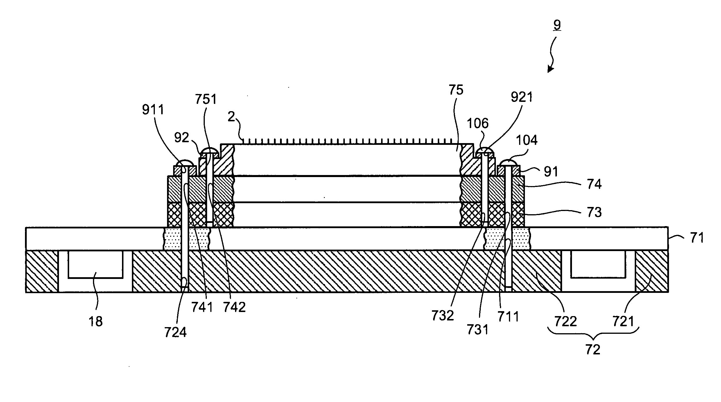
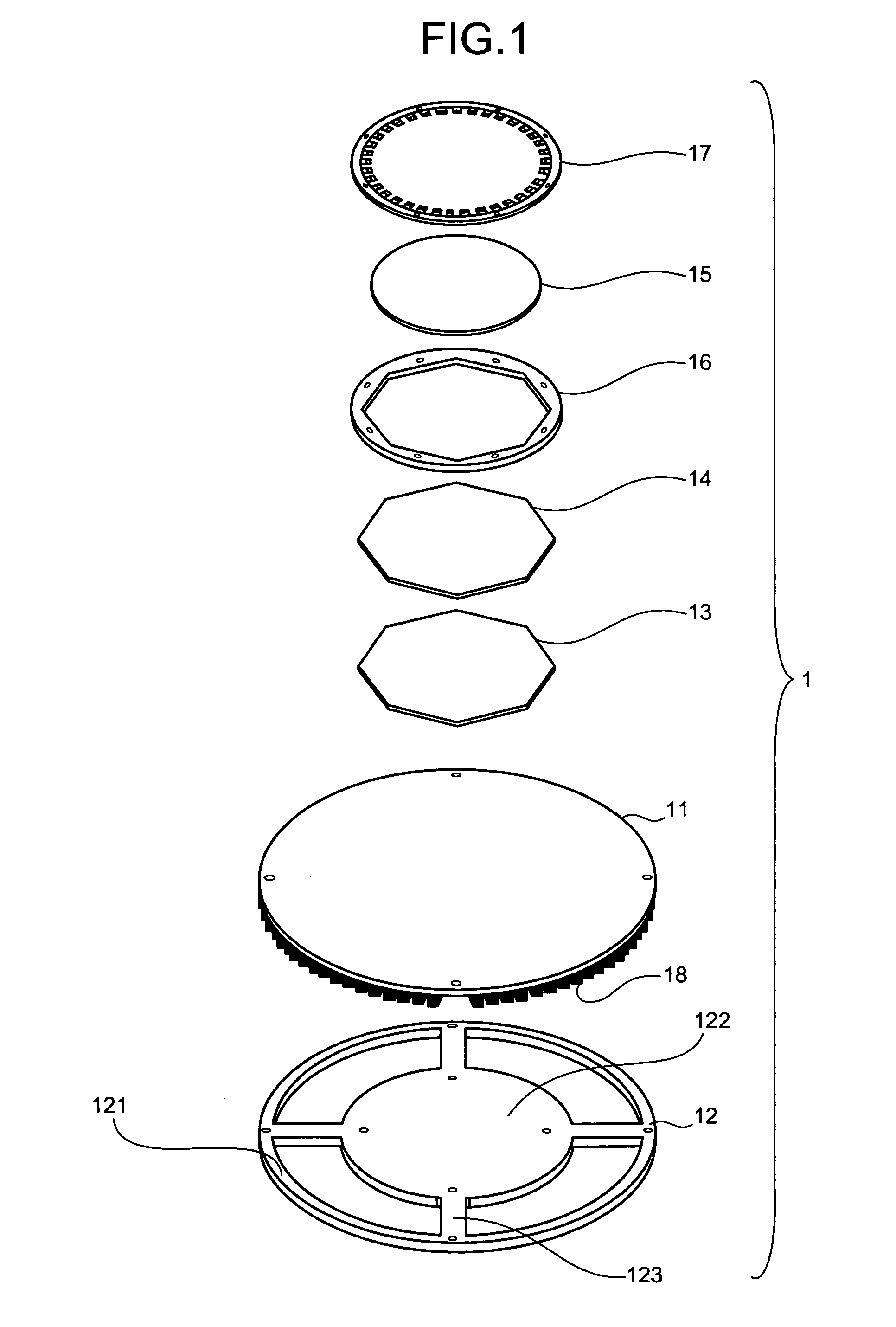
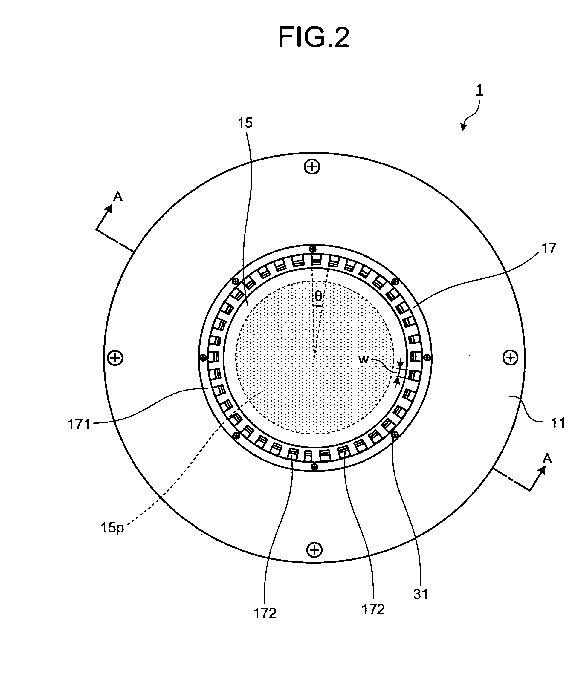
[0079]FIG. 1 is an exploded perspective view of a structure of a relevant part of a probe card according to a first embodiment of the present invention. FIG. 2 is a plan view of the probe card according to the first embodiment when viewed from the top in FIG. 1. FIG. 3 is a relevant part cross sectional view taken along line A-A in FIG. 2. A probe card 1 shown in FIGS. 1 to 3 electrically connects, using a plurality of probes, a semiconductor wafer as a test object and a testing device including a circuit structure that generates a signal for a test.

[0080]The probe card 1 includes a substrate 11 that is formed in a disc shape and realizes electrical connection with the testing device, a reinforcing member 12 that is mounted on one side of the substrate 11 and reinforces the substrate 11, an interposer 13 for connection of wires from the substrate 11, which has a regular octagonal surface and is formed in a thin plate shape, a space transformer 14 that transforms intervals between th...

modification example of first embodiment

[0118]FIG. 9 is a partial cross sectional view of a structure of a relevant part of a probe card according to a modification example of the first embodiment. A probe card 4 shown in FIG. 9 is different from the first embodiment in the shape of the leaf spring.

[0119]A leaf spring 19 includes an annular thin outer peripheral portion 191 and pawl portions 192 that extend in the inner circumference direction from the outer peripheral portion 191. The pawl portion 192 has a V-shape in cross section with approximately a central portion of a portion extending from the outer peripheral portion 191 as an apex. A contact surface that is positioned on the inner circumference side of the apex and is in contact with the space transformer 14 is approximately parallel to the surface of the outer peripheral portion 191 in the state where the probe head 15 is attached and has a level difference with respect to the outer peripheral portion 191. The pawl portion 192 is applied with a load in advance i...

second embodiment

[0121]FIG. 10 is an exploded perspective view of a structure of a relevant part of a probe card according to a second embodiment of the present invention. FIG. 11 is a partial cross sectional view of a structure of a relevant part of the probe card according to the second embodiment. A probe card 5 shown in FIGS. 10 and 11 has a structure in which a plurality of post members 54 is embedded in a plurality of hole portions 511 provided at predetermined positions in a substrate 51.

[0122]The post member 54 includes a hollow cylindrical large diameter portion 54a having a thickness slightly larger than a thickness of the substrate 51 and a small diameter portion 54b that has a smaller diameter than the large diameter portion 54a and a center axis same as the large diameter portion 54a. A hollow portion 541 is provided in the center axis direction (height direction) in the post member 54. The hollow portion 541 communicates with hole portions 524 and 531 formed in a reinforcing member 52 ...


PUM


Abstract

A probe card is provided that is capable of accurately ensuring the flatness and the parallelism with respect to a predetermined reference surface. A point (Q) of application of force applied from a leaf spring (17) that presses a portion near an edge portion of a surface of a probe head (15) from which a plurality of probes projects over an entire circumference in a direction of a substrate to the probe head (15) is positioned inside of an outer edge of the probe head (15), and a point (P) of application of force applied from the retainer (16) that presses a portion near an edge portion of a space transformer (14) over an entire circumference in the direction of the substrate to the space transformer (14) is positioned inside of an outer edge of the space transformer (14).

Description

TECHNICAL FIELD[0001]The present invention relates to a probe card that electrically connects a semiconductor wafer as a test object and a circuit structure that generates a signal for a test.BACKGROUND ART[0002]In a semiconductor test process, a wafer level test for detecting a defective product is sometimes performed by performing a conductivity test by bringing probes having conductivity (conductive probes) into contact with a semiconductor wafer before dicing. When the wafer level test is performed, to transfer a signal for a test generated and sent by a testing device (tester) to the semiconductor wafer, a probe card housing a large number of probes is used. In the wafer level test, the probes are individually brought into contact with each of dies on the semiconductor wafer while the dies are scanned by the probe card. However, because hundreds to tens of thousands of dies are formed on the semiconductor wafer, it takes considerable time to test one semiconductor wafer. Thus, ...

Claims


Application Information

Patent Timeline
Patent Type & Authority Applications(United States)
IPC IPC(8): G01R31/02G01R31/26
CPCG01R1/07314G01R1/07371G01R31/2889G01R1/06722
Inventor YAMADA, YOSHIONAKAYAMA, HIROSHINAGAYA, MITSUHIROINUMA, TSUYOSHIAKAO, TAKASHI
Owner NHK SPRING CO LTD
Why Eureka
Try Eureka