Semiconductor memory device, host device and semiconductor memory system

a memory device and semiconductor technology, applied in the direction of memory address formation, memory allocation/allocation/relocation, instruments, etc., can solve the problems of data not being disadvantageously recovered and data being impossible to recover, so as to prevent data destruction, eliminate the effect of error propagation, and be highly reliabl

Active Publication Date: 2010-07-08
PANASONIC CORP
View PDF11 Cites 10 Cited by
  • Summary
  • Abstract
  • Description
  • Claims
  • Application Information

AI Technical Summary

Benefits of technology

[0039]The semiconductor memory system according to the present invention is provided with a data release determinator to release data in the data buffer in units of the predetermined blocks when data transfer in units of the predetermined blocks is completed. Thereby, even when error propagation accompanying the cell sharing occurs, writing can be performed again using the data in the data buffer, thereby enabling prevention of data destruction due to the error propagation.
[0040]Furthermore, according to the claims 4, 5, 12 and 13 of the present invention, the host device is provided with the new block writing request part and when writing is performed in a case where the host device does not hold data in a cell sharing part, the new block writing request part expressly requests writing to a new block to the semiconductor memory device and allows writing data to a newly secured block. Thereby, it is possible to provide a highly reliable semiconductor memory system which eliminates an effect of the error propagation due to the cell sharing.

Problems solved by technology

For this reason, disadvantageously, there are cases that retry cannot be performed and thus, data recovery is impossible.
When power disconnection suddenly occurs during data writing, even if data for recovery is held, retry itself cannot be performed, resulting in that the data cannot be disadvantageously recovered.

Method used


Image

  • Semiconductor memory device, host device and semiconductor memory system
  • Semiconductor memory device, host device and semiconductor memory system
  • Semiconductor memory device, host device and semiconductor memory system

Examples


first embodiment

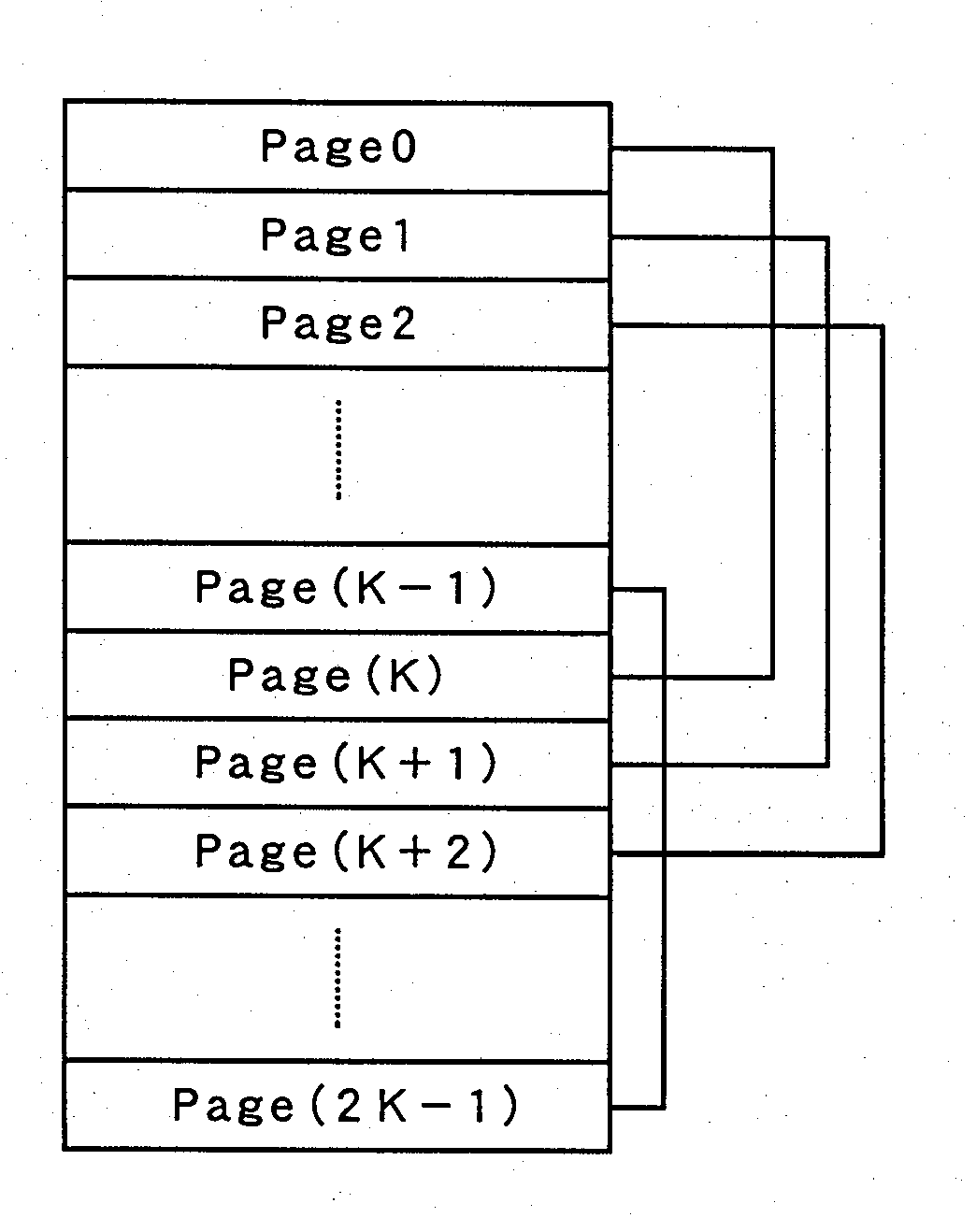
[0067]FIGS. 6A and 6B are configuration diagrams showing a semiconductor memory system in accordance with a first embodiment of the present invention. The semiconductor memory system includes a semiconductor memory device 100A and host device 200A. The semiconductor memory device 100A stores data therein according to a write command from the host device 200A, and reads data according to a read command and sends the data to the host device 200A. The host device 200A controls the semiconductor memory device 100A and performs data writing and data reading.

[0068]Next, each block in the semiconductor memory device 100A in the present embodiment will be described referring to FIG. 6A. An external interface 110 is an interface for receives a command and data from the host device 200A and transferring the data.

[0069]An address converter 120 converts a logical address at which the host device 200A request data reading / writing to an address of a physical memory in the semiconductor memory dev...

second embodiment

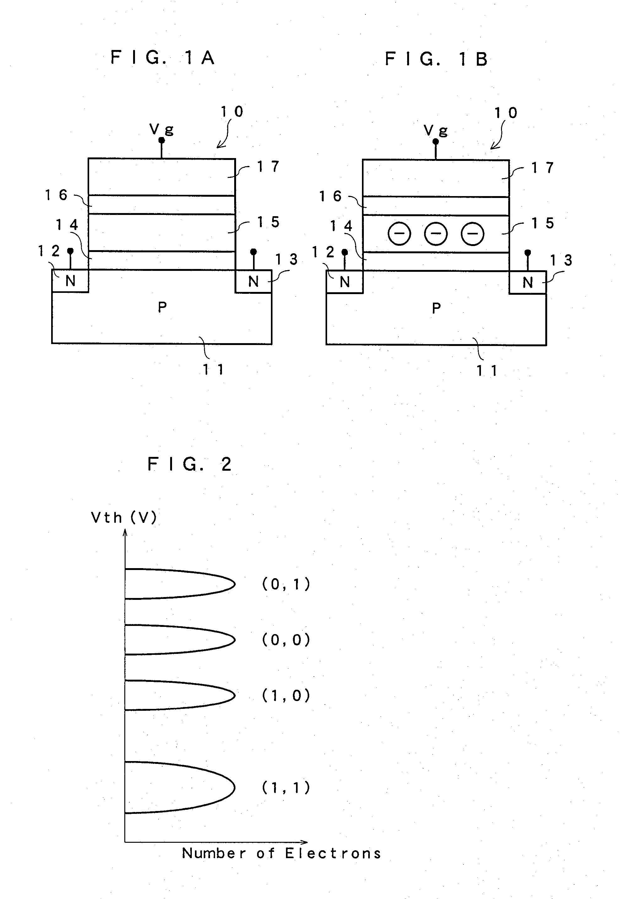
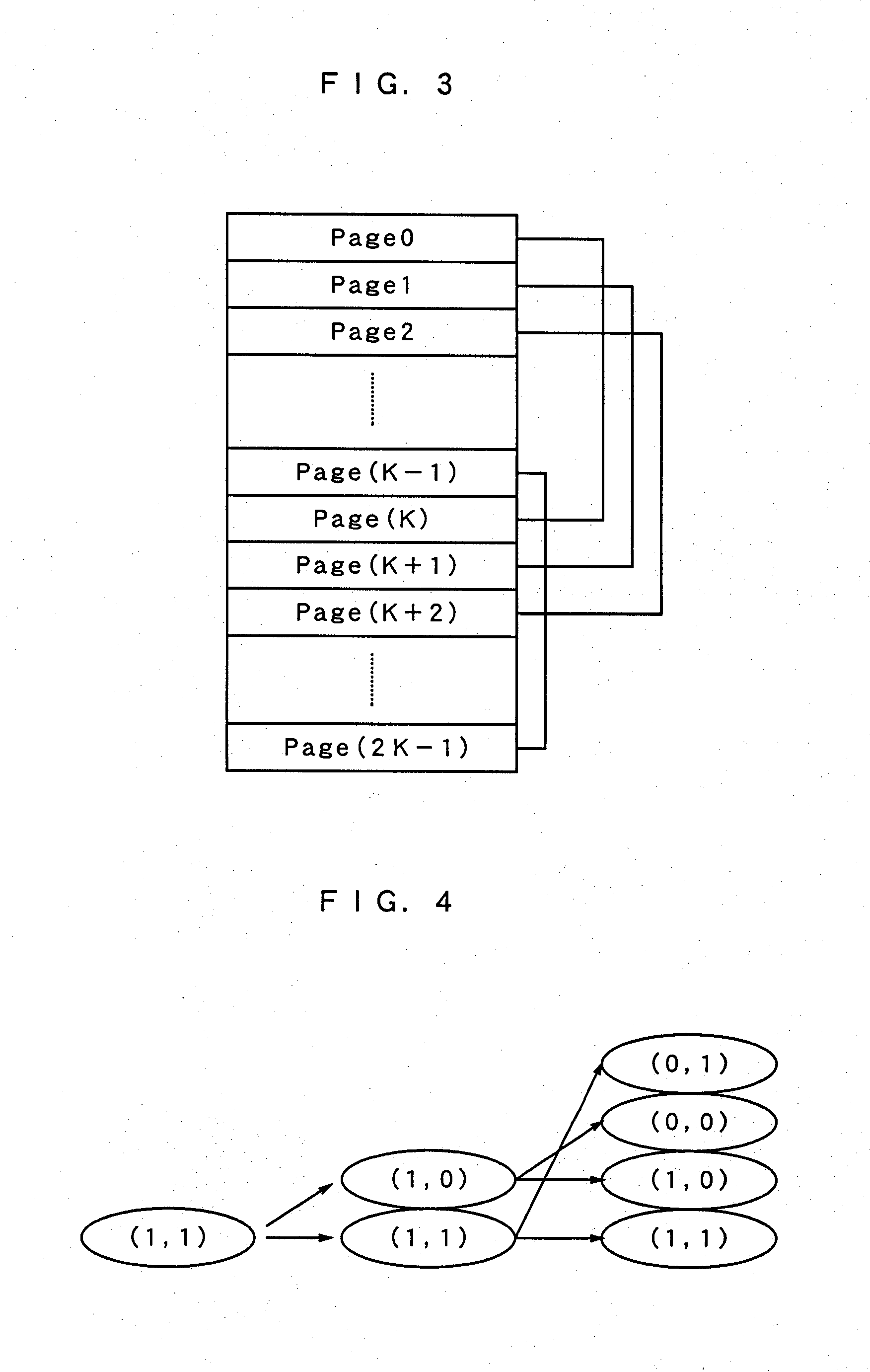
[0107]Next, the second embodiment of the present invention will be described. FIG. 19A shows a configuration of a semiconductor memory device 100B in accordance with a second embodiment and FIG. 19B shows a configuration of a host device 200B. As shown in FIG. 19A, in the semiconductor memory device 100B, an error propagation detector 190 is connected to the data writer 130. The error propagation detector 190 determines whether or not data is written to a second page of the flash memory and an error can propagate as a result of the writing, and when the error actually occurs, the error propagation detector 190 informs error propagation possibility to the host device 200B through the external interface 110. In a case of receiving the error propagation possibility through the external interface 210, a command issuer 280 of the host device 200B issues a command to rewrite data in unit of physical blocks. The other operation of the command issuer 280 is the same as that of the command i...


PUM


Abstract

A host device 200A includes a data buffer 250. When data has been already written to a part of a physical block and data is additionally written to the physical block, it is determined whether or not the data written to the physical block is held in the data buffer. When the data is held, data is written to the block, and when an error exists, data in unit of physical blocks is rewritten. When the data is not held in the data buffer, a new physical block is required to be secured and then, data is written to the new block. Thereby, even when power is shut off or an error occurs during writing in the semiconductor memory device, destruction of data already written is prevented.

Description

BACKGROUND OF THE INVENTION[0001]1. Field of the Invention[0002]The present invention relates to a semiconductor memory device such as a memory card, host device and semiconductor memory system, in particular, to a technique for recovering a writing error occurring in a nonvolatile memory within the semiconductor memory device.[0003]2. Discussion of the Related Art[0004]Conventionally, a semiconductor memory device such as an SD (Secure Digital) card as a card-type recording medium which has a flash memory therein is very small and thin and due to its handiness, is widely used for recording data such as images in a digital camera, portable equipment and so on.[0005]The flash memory contained in the semiconductor memory device is a nonvolatile memory which can erase and rewrite data in units of block of a uniform size. To address a demand for an increase in capacity in recent years, the flash memory capable of storing data of two bits or more in one cell has been commercialized.[0006...

Claims


Application Information

Patent Timeline
Patent Type & Authority Applications(United States)
IPC IPC(8): G06F11/16G06F12/00G06F12/10G06F12/02
CPCG06F12/0246G06F2212/7202G06F2212/1032
Inventor YAMASHITA, HIDEAKIOOTSUKA, TAKESHI
Owner PANASONIC CORP
Why Eureka
Try Eureka