Semiconductor integrated circuit device and operating method thereof

a technology of integrated circuit and integrated circuit device, which is applied in the direction of information storage, static storage, digital storage, etc., can solve the problems of miniaturization and increase in local delay fluctuations in the semiconductor manufacturing process, and achieve the effect of reducing the generating timing of the sense-amplifier

Active Publication Date: 2010-07-15
RENESAS ELECTRONICS CORP
View PDF5 Cites 28 Cited by
  • Summary
  • Abstract
  • Description
  • Claims
  • Application Information

AI Technical Summary

Benefits of technology

[0019]Therefore, an object of the present invention is to reduce the fluctuations of the generating timing of the sense-amplifier enable signal even when the memory capacity of the semiconductor memory that uses the replica bit-lines (RBL) built in the semiconductor integrated circuit device is made higher.
[0024]The above typical embodiment has the feature that by the sense-amplifier enable signal (sae) being supplied to the plurality of sense-amplifiers (SA), a plurality of read signals of the plurality of bit-lines are amplified by the plurality of sense-amplifiers, and a plurality of pieces of read data (q[0] to q[m]) are generated from a plurality of output terminals of the sense-amplifiers (see FIG. 4). Effects obtained by typical one of the inventions disclosed in the present application will be briefly described as follows. That is, the fluctuations of the generating timing of the sense-amplifier enable signal can be reduced even if the memory capacity of the semiconductor memory that uses the replica bit-lines (RBL) is made higher.

Problems solved by technology

Meanwhile, local delay fluctuations in the semiconductor manufacturing process increase for the miniaturization of the process.

Method used


Image

  • Semiconductor integrated circuit device and operating method thereof
  • Semiconductor integrated circuit device and operating method thereof
  • Semiconductor integrated circuit device and operating method thereof

Examples


first embodiment

[First Embodiment]

[0078]>

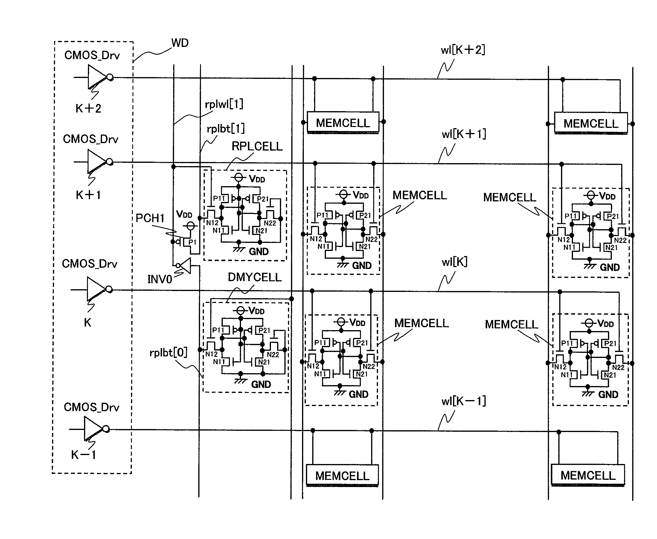
[0079]FIG. 3 is a view showing a configuration of a SRAM that uses replica bit-lines according to a first embodiment of the present invention.

[0080]The SRAM shown in FIG. 3 is basically different from the SRAM shown in FIG. 1 in that one replica bit-line rplbt of the SRAM shown in FIG. 1 is divided into a plurality of replica bit-lines rplbt[0] and rplbt[1] as shown in the SRAM of FIG. 3, whereby delay amounts at the replica bit-lines are reduced.

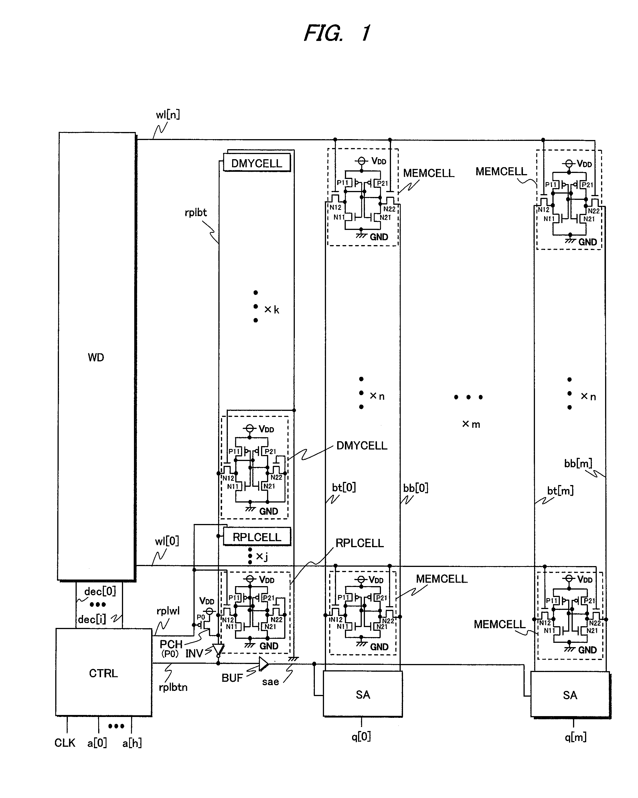
[0081]Similarly to the SRAM shown in FIG. 1, the SRAM shown in FIG. 3 also includes: a word driver (WD); a decode control circuit (CTRL); a plurality (n+1>1) of word lines (wl[0] to [n]); a plurality (m+1>1) of bit-line / inverted-bit-line pairs (bt[0], bb[0] to bt [m], bb[m]); a plurality ((n+1)×(m+1)) of SRAM memory cells (MEMCELKL); and a plurality (m+1>1) of sense-amplifiers (SA).

[0082]The SRAM shown in FIG. 3 is different from the SRAM shown in FIG. 1 in that the SRAM shown in FIG. 3 includes: a first replica wor...

third embodiment

[0102]A third embodiment of the present invention forms the inverters INV0 and INV1, and the pre-charge transistors PCH0 and PCH1 of the replica bit-lines rplbt [0] and [1], all of which are included in the SRAM of the first embodiment, by using the SRAM memory cells MEMCELL, the replica memory cells RPLCELL, and the dummy memory cells DMYCELL.

[0103]FIG. 7 is a view showing a configuration of a SRAM according to a third embodiment of the present invention.

[0104]The inverters INV0 and INV1 included in the SRAM of the first embodiment shown in FIG. 3 are replaced by an inverter cell (INVCELL) 701 of the SRAM of the third embodiment shown in FIG. 7; and the pre-charge transistors PCH0 and PCH1 included in the SRAM of the first embodiment shown in FIG. 3 are replaced by a pre-charge cell (PCHCELL) 702 of the SRAM of the third embodiment shown in FIG. 7. Note that the SRAM of the third embodiment shown in FIG. 7 includes a dummy memory cell (DMYCELL) 703, and a replica memory cell (RPLCE...

fourth embodiment

[0109]A fourth embodiment of the present invention adjusts a load capacity of each of the replica bit-lines rplbt [0] and [1] by changing a connection state of a transistor node of the dummy memory cell (DMYCELL) 703 included in the SRAM of the third embodiment shown in FIG. 7.

[0110]FIG. 10 is a view showing a configuration of a dummy memory cell (DMYCELL) 703 included in a SRAM according to a fourth embodiment of the present invention.

[0111]The dummy memory cell (DMYCELL) 703 shown in FIG. 10 includes two P-channel MOS transistors pll100 and plr100 and four N-channel MOS transistors npl100, ndl100, ndr100, and npr100. In the dummy memory cell (DMYCELL) 703 shown in FIG. 10, a drain of the N-channel MOS transistor nprl100 in addition to the drain of the N-channel MOS transistor npll100 is connected to a replica bit-line rplbt [0], whereby load capacity of the replica bit-line rplbt [0] can be increased.

[0112]FIG. 11 is also a view showing the configuration of the dummy memory cell (...


PUM


Abstract

Even when memory capacity of a memory that uses a replica bit-line is made higher, fluctuations of a generating timing of a sense-amplifier enable signal are reduced. A semiconductor integrated circuit device comprises a plurality of word lines, a plurality of bit-lines, a plurality of ordinary memory cells, an access control circuit, a plurality of sense-amplifiers, first and second replica bit-lines, first and second replica memory cells, and first and second logic circuits. The first and second replica memory cells are connected to the first and second replica bit-lines, respectively; inputs of the first and second logic circuits are connected to the first and second replica bit-lines, respectively; a sense-amplifier enable signal is generated from an output of the second logic circuit; and this signal is supplied to a plurality of sense-amplifiers.

Description

CROSS-REFERENCE TO RELATED APPLICATION[0001]The present application claims priority from Japanese Patent Application No. JP 2009-006887 filed on Jan. 15, 2009, the content of which is hereby incorporated by reference into this application.TECHNICAL FIELD OF THE INVENTION[0002]The present invention relates to a semiconductor integrated circuit device and its operating method, and particularly relates to a technique useful for reducing fluctuations (changes or variations) of a generating timing of a sense-amplifier enable signal even when memory capacity of a built-in semiconductor memory using replica bit-lines (RBL) is made higher.BACKGROUND OF THE INVENTION[0003]To achieve high-speed, low-power read operations of Static Random Access Memories (SRAM) built in the semiconductor integrated circuit device, small-amplitude bit-lines (BL) and clocked sense-amplifiers are employed. For the reliable operation at high-speed, however, the sense-amplifier enable (SAE) signal must track delay ...

Claims


Application Information

Patent Timeline
Patent Type & Authority Applications(United States)
IPC IPC(8): G11C7/00G11C7/02
CPCG11C7/08G11C11/413G11C7/227G11C7/22
Inventor KOMATSU, SHIGENOBUYAMAOKA, MASANAOMAEDA, NORIAKIMORIMOTO, MASAOSHIMAZAKI, YASUHISA
Owner RENESAS ELECTRONICS CORP
Why Eureka
Try Eureka