Semiconductor device and manufacturing method of the semiconductor device

a semiconductor device and semiconductor technology, applied in semiconductor devices, semiconductor/solid-state device details, electrical devices, etc., can solve the problems of reducing yield, increasing mounting area, increasing cost, etc., and achieve the effect of preventing voids, improving connection reliability of semiconductor devices and yield

Active Publication Date: 2010-07-22
SONY CORP
View PDF5 Cites 5 Cited by
  • Summary
  • Abstract
  • Description
  • Claims
  • Application Information

AI Technical Summary

Benefits of technology

[0021]According to the embodiments of the invention, in the semiconductor device having the structure in which the semiconductor chip is mounted on the mounted body, the climbing of the underfill material onto the semiconductor chip and the occurrence of voids can be prevented. Thus, the connection reliability of the semiconductor device and the yield can be improved.

Problems solved by technology

With improvement in integration, performance and function of LSIs, problems such as reduction in yield, increase in mounting area, and increase in cost become serious.

Method used


Image

  • Semiconductor device and manufacturing method of the semiconductor device
  • Semiconductor device and manufacturing method of the semiconductor device
  • Semiconductor device and manufacturing method of the semiconductor device

Examples


first embodiment

2. First Embodiment

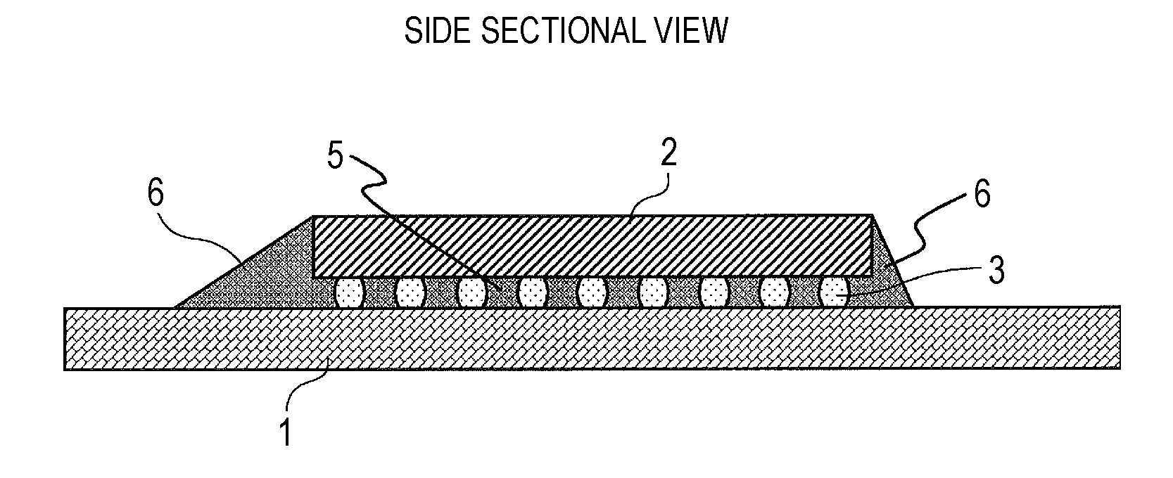
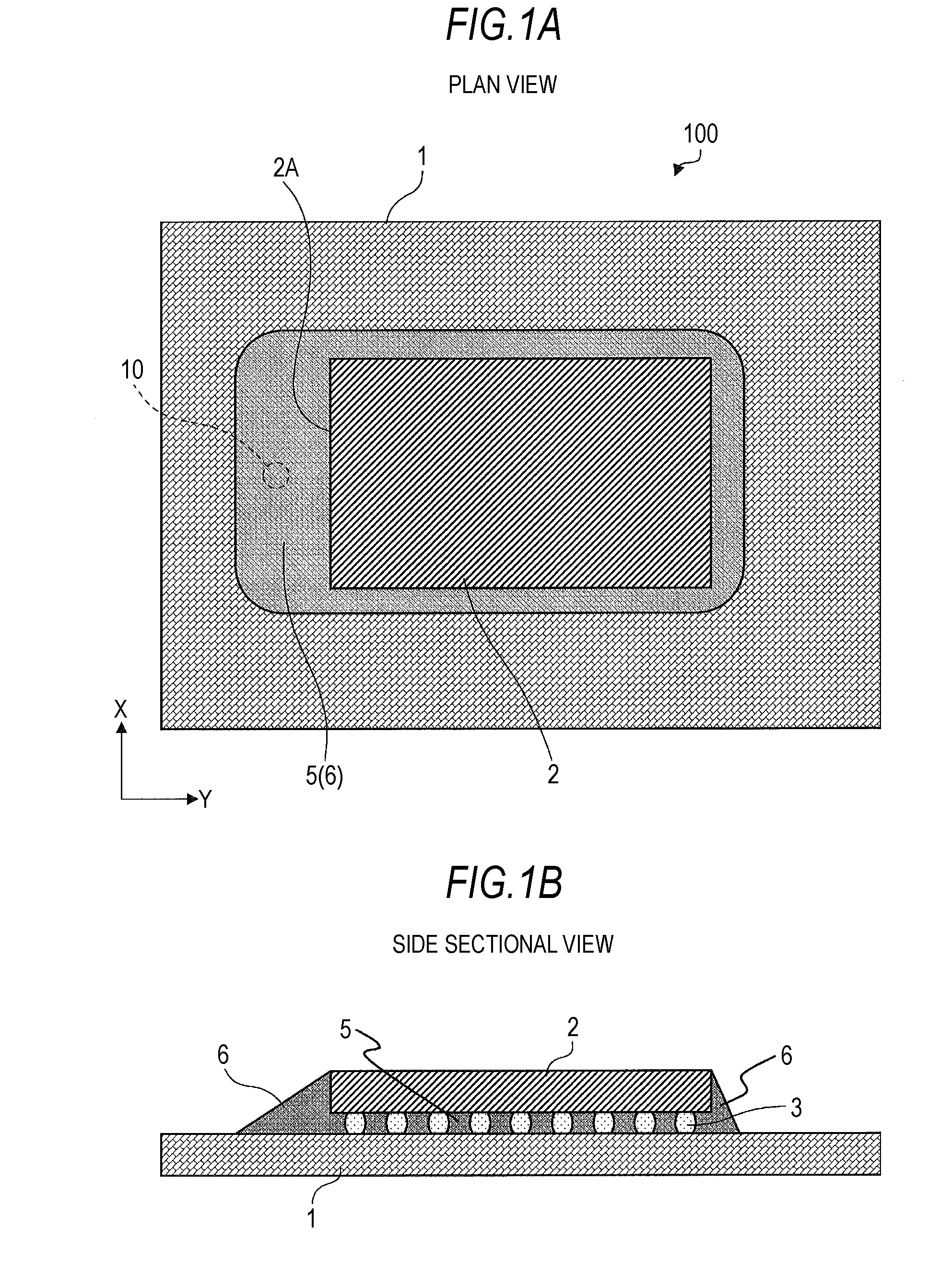
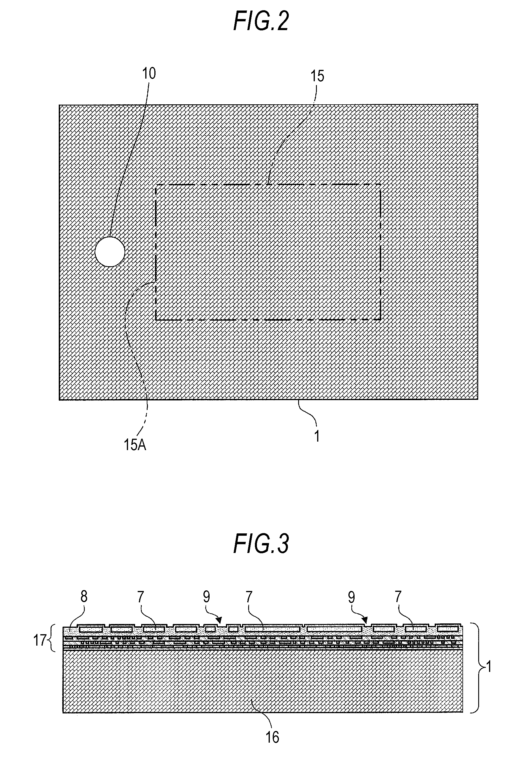
[0065]FIG. 4 is a plan view showing a structure of a semiconductor device of a first embodiment of the invention, in which a part of a device formation surface of a first semiconductor chip 1 before a second semiconductor chip 2 is mounted is enlarged. FIG. 5 is a J-J sectional view of FIG. 4. As shown in the drawings, a chip mount area 15 is set in the device formation surface of the first semiconductor chip 1. The chip mount area 15 is defined in conformity to the outer shape of the second semiconductor chip 2 and is formed into a quadrangle when viewed in plane. A supply area 10 of an underfill material is set in the vicinity of one side section 15A of four side sections defining the chip mount area 15. Plural wiring patterns 7 are formed in a direction parallel to the side section 15A of the chip mount area 15 and on the inside and the outside of the chip mount area 15. The respective wiring patterns 7 form the wiring layer of the uppermost layer of the multi-...

second embodiment

3. Second Embodiment

[0074]FIG. 9 is a plan view showing a structure of a semiconductor device of a second embodiment of the invention, in which a part of a device formation surface of a first semiconductor chip 1 before a second semiconductor chip 2 is mounted is enlarged. This second embodiment is different from the first embodiment in the structure of an injection section 18. That is, the injection section 18 is disposed on the outside of a chip mount area 15 set on a first semiconductor chip 1 and in a state where a part of one wiring pattern 7 closest to a side section 15A of the chip mount area 15 is cut away in a slit shape. Similarly to the first embodiment, the injection section 18 is formed on the outside of the side section 15A of the chip mount area 15 on which a fillet 6 is formed to be longest. Besides, similarly to the first embodiment, the injection section 18 is formed in the slit shape and in a direction crossing the wiring direction of the wiring pattern 7. One end...

third embodiment

4. Third Embodiment

[0076]FIG. 10 is a plan view showing a structure of a semiconductor device of a third embodiment of the invention, in which a part of a device formation surface of a first semiconductor chip 1 before a second semiconductor chip 2 is mounted is enlarged. This third embodiment is different from the second embodiment in a positional relation between a side section 15A of a chip mount area 15 and an injection section 18. That is, in the second embodiment, the one end of the injection section 18 is positioned in conformity with the side section 15A of the chip mount area 15 and is disposed. However, in the third embodiment, the injection section 18 is disposed in the state where it crosses the side section 15A of the chip mount area 15. The form in which the injection section 18 crosses the side section 15A of the chip mount area 15 is realized by disposing, in the Y direction, one end of the injection section 18 on the inside of the chip mount area 15 and disposing th...


PUM


Abstract

A semiconductor device includes: a mounted body in which a wiring pattern is formed on a first main surface; a semiconductor chip mounted on the surface of the mounted body on which the wiring pattern is formed; an underfill material which is filled between the mounted body and the semiconductor chip and forms a fillet on an outer peripheral part of the semiconductor chip; and an injection section which is disposed on the mounted body and on an outside of a side section, on which the fillet is formed to be longest, of four side sections defining a chip mount area on which the semiconductor chip is mounted, and guides the underfill material to between the mounted body and the semiconductor chip.

Description

BACKGROUND OF THE INVENTION[0001]1. Field of the Invention[0002]The present invention relates to a semiconductor device and a manufacturing method of the semiconductor device. More particularly, the present invention relates to a semiconductor device having a structure in which a semiconductor chip is mounted on a mounted body and a manufacturing method of the same.[0003]2. Description of the Related Art[0004]With improvement in integration, performance and function of LSIs, problems such as reduction in yield, increase in mounting area, and increase in cost become serious. In recent years, attention is paid to SiP (System in Package) in which both these problems and the LSI performance can be managed. The SiP can be classified into various structures such as a package lamination type, a chip stack type, and a chip-on-chip type, and particularly, the chip-on-chip type is advantageous in speedup and reduction in consumed electric power since chips can be multi-pin connected to each o...

Claims


Application Information

Patent Timeline
Patent Type & Authority Applications(United States)
IPC IPC(8): H01L23/16H01L21/56H01L23/488
CPCH01L2924/01019H01L2224/73203H01L2224/16225H01L2224/32225H01L21/563H01L2924/01012H01L2224/73204H01L2924/00H01L2224/05567H01L2224/05573H01L2924/00014H01L2224/0554H01L2224/92125H01L2224/05599H01L2224/0555H01L2224/0556
Inventor HARADA, YOSHIMICHIMURAI, MAKOTOTANAKA, TAKAYUKINAKAMURA, TAKUYA
Owner SONY CORP
Why Eureka
Try Eureka