Solid-state imaging element and method for manufacturing the same

a technology of solid-state imaging and manufacturing methods, applied in the direction of material analysis, radio frequency control devices, instruments, etc., can solve the problems of insufficient approach for subpixels of about 0.9 m in size, and achieve the effect of enhancing positioning accuracy and preventing sensitivity and color mixing

Inactive Publication Date: 2011-06-16
SONY CORP
View PDF4 Cites 3 Cited by
  • Summary
  • Abstract
  • Description
  • Claims
  • Application Information

AI Technical Summary

Benefits of technology

[0005]In, for example, Japanese Unexamined Patent Application Publication No. 9-148549, the reduction of sensitivity and the color mixing are prevented by increasing the light-concentration efficiency using on-chip microlenses. However, this approach is not sufficient for subpixels of about 0.9 μm in size.
[0006]Accordingly, it is desirable to provide a solid-state imaging element that can certainly prevent the reduction of sensitivity and the occurrence of color mixing even if the size of subpixels (light-receiving element portions) is reduced, and a method for manufacturing the same.
[0009]In the solid-state imaging element of the embodiments of the present invention, an antenna structure surrounded by an insulating layer is provided on the light-receiving element portion. The antenna structure is made of a material having a refractive index higher than that of the material of the insulating layer. Accordingly, the energy of light entering the antenna structure and the insulating layer is concentrated in the light-receiving element portion. Consequently, the sensitivity and the occurrence of color mixing can be certainly prevented even if the size of the light-receiving element portion is reduced. The structure disposed on the light-receiving element portion is called an antenna structure because it concentrates light energy in the light-receiving element portion. In the method for manufacturing the solid-state imaging element, the presence of the light-shielding layer allows the antenna structure surrounded by the insulating layer (second insulating layer) to be formed in a self-aligned manner. This can enhance the accuracy in positioning when the insulating layer (second insulating layer) and the antenna structure are formed.

Problems solved by technology

However, this approach is not sufficient for subpixels of about 0.9 μm in size.

Method used


Image

  • Solid-state imaging element and method for manufacturing the same
  • Solid-state imaging element and method for manufacturing the same
  • Solid-state imaging element and method for manufacturing the same

Examples


first embodiment

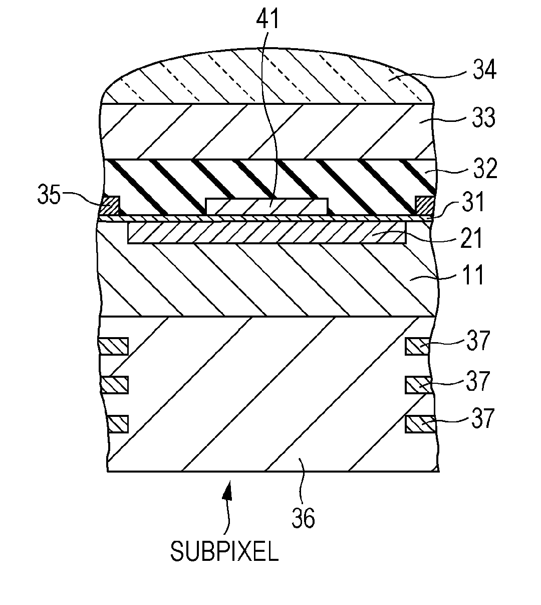
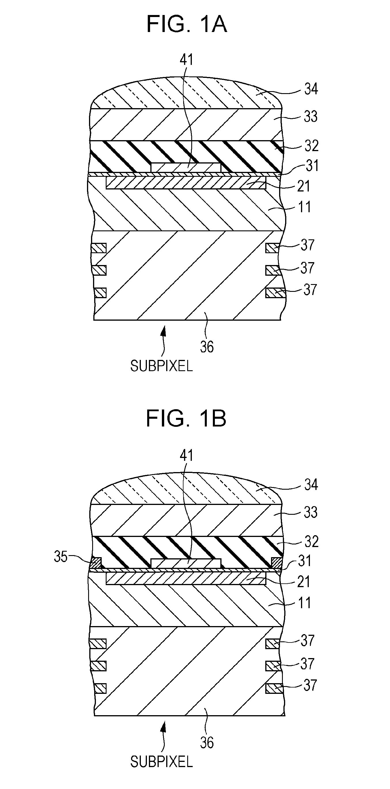
[0049]In a first embodiment, a solid-state imaging element will be described. FIG. 1A is a schematic fragmentary sectional view of a solid-state imaging element according to the first embodiment. The solid-state imaging element is of rear emission type, and includes (A) a light-receiving element portion 21 formed in a semiconductor layer 11, (B) an insulating layer 32 disposed over the semiconductor layer 11, and (C) an antenna structure 41 disposed over the light-receiving element portion 21 and enclosed in the insulating layer 32.

[0050]In the solid-state imaging element of the present embodiment, an insulating interlayer (not shown) is formed over the antenna structure 41 and the insulating layer 32. Although the insulating interlayer is not necessarily provided, it is preferably provided from the viewpoint of enhancing the adhesion of a color filter. The color filter (on-chip color filter) 33 is formed on the insulating interlayer, and a microlens (on-chip microlens) 34 is dispos...

second embodiment

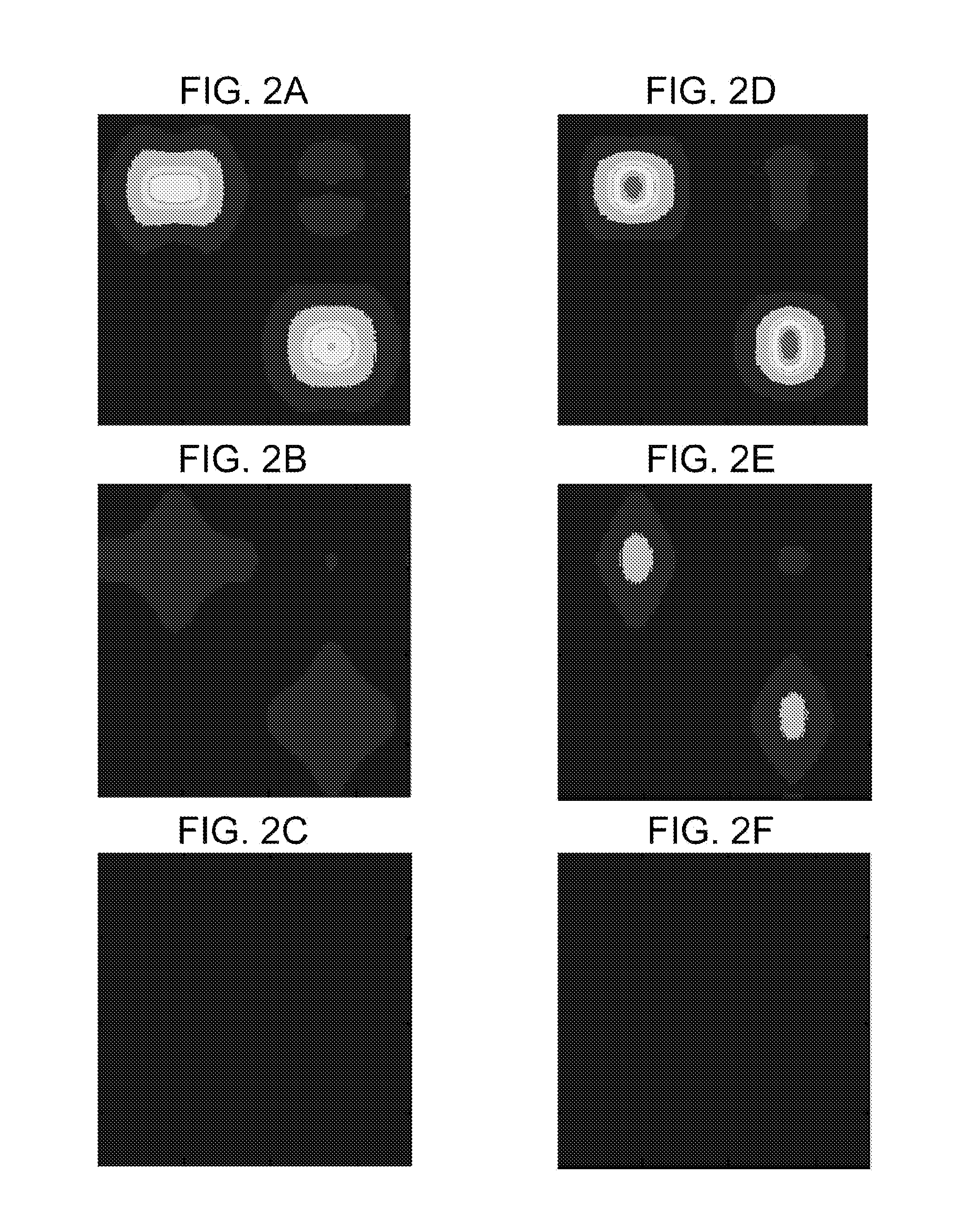
[0067]In a second embodiment, the solid-state imaging element of the first embodiment is modified. For the second embodiment, the red color mixing ratios were measured of solid-state imaging elements including the disc-like antenna structures 41 having different diameters R1 and heights H1. The results are shown in FIG. 3A. In FIG. 3A, data A indicated by black squares represents the results of samples each including the antenna structure having a height H1 of 0.2 μm; data B indicated by black rhombuses represents the results of samples each including the antenna structure having a height H1 of 0.1 μm; and data C indicated by black triangles represents the results of samples each including the antenna structure having a height H1 of 0.5 μm. As shown in FIG. 3A, the antenna structure 41 can have a diameter R1 of 0.2 to 0.4 μm, more preferably 0.2 to 0.3 μm. Preferably, the antenna structure 41 is in a columnar shape, and its section taken in the direction perpendicular to the height ...

third embodiment

[0069]In a third embodiment, the solid-state imaging element of the first embodiment is modified. In the third embodiment, a tungsten (W) light-shielding layer 35 is provided around the antenna structure 41 with the insulating layer 32 therebetween, as shown in the schematic fragmentary sectional view of FIG. 1B. More specifically, the antenna structure 41 is surrounded by a ring-shaped light-shielding layer 35 in such a manner that they are separated by the insulating layer 32. Samples of the solid-state imaging element according to the third embodiment were prepared. In the samples, the ring-shaped light-shielding layer 35 had a height of 0.2 μm and a width (thickness) of 0.2 μm, and the distance between the side surface of the antenna structure 41 and the side surface of the light-shielding layer 35 was 0.15 μm. The antenna structure 41 had a height H1 of 0.2 μm. The red color mixing ratios were measured of the samples including disc-like antenna structures 41 having different di...


PUM


Abstract

A solid-state imaging element includes a light-receiving element portion disposed in a semiconductor layer, an insulating layer made of a material having a refractive index n0, disposed over the semiconductor layer, and an antenna structure disposed over the light-receiving element portion and surrounded by an insulating layer. The antenna structure is made of a material having a refractive index higher than the refractive index of the insulating layer. The energy of light having entered the antenna structure and the insulating layer is concentrated in the light-receiving element portion.

Description

BACKGROUND OF THE INVENTION[0001]1. Field of the Invention[0002]The present invention relates to a solid-state imaging element and a method for manufacturing the same.[0003]2. Description of the Related Art[0004]In semiconductor image sensors represented by CMOS image sensors, it is desirable that the sizes of the subpixels constituting a pixel, including a subpixel receiving red light, a subpixel receiving green light and a subpixel receiving blue light, is reduced to increase the number of pixels in an image area. However, the increase of the number of pixels reduces the size of the pixels, and reduces the size of light-receiving element portions of the subpixels accordingly. Consequently, the sensitivity of the light-receiving element portion is reduced to make it difficult to ensure a desired signal-to-nose (S / N) ratio. In addition to the reduction of the sensitivity, color mixing, which is a phenomenon in which incident light leaks to the light-receiving element portion in the ...

Claims


Application Information

Patent Timeline
Patent Type & Authority Applications(United States)
IPC IPC(8): H01L31/0232H01L27/146H01L31/18
CPCH01L27/14621H01L27/14625H01L27/14689H01L27/14645H01L27/14685H01L27/14627
Inventor KIKUCHI, KOJI
Owner SONY CORP
Why Eureka
Try Eureka