Semiconductor device

Active Publication Date: 2010-08-05
PANASONIC CORP
View PDF4 Cites 21 Cited by
  • Summary
  • Abstract
  • Description
  • Claims
  • Application Information

AI Technical Summary

Benefits of technology

[0046]According to the present invention, in a semiconductor device that has a multilayer structure including first and second semiconductor layers on an off-cut semiconductor substrate, the margin (i.e., the difference in length) is increased in the off-cut direction either between the second semiconductor layer and the second conductor or between the conductive surface of the first conductor and the first conductive region. Then, even if any misalignment has occurred due to a decrease in the recognizability of an alignment pattern caused by the deposition of the second semiconductor layer, various kinds of deterioration in device characteristics, including short-circuit or contact failure between electrodes and an increase in ON-state resistance, can be minimized. As a result, a highly reliable semiconductor device can be pro

Problems solved by technology

If a semiconductor film is grown as that another film on the semiconductor layer 12 with those markers 121, however, the markers could get blunted, and could become difficult to recognize, according to the method of growing that semiconductor film.
If such recesses 122 were used as markers in a photolithographic process step to be carried out after the extra-

Method used


Image

  • Semiconductor device
  • Semiconductor device
  • Semiconductor device

Examples


embodiment 1

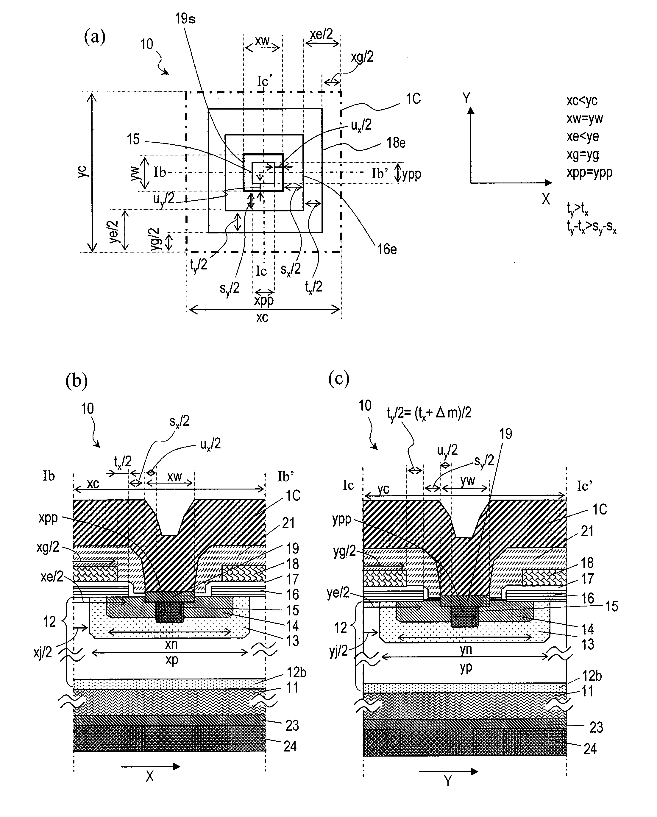
[0065]Hereinafter, a first preferred embodiment of a semiconductor device according to the present invention will be described with reference to FIGS. 1 and 2. The semiconductor device of this preferred embodiment is a vertical MOSFET that has been fabricated on an off-cut semiconductor substrate, and typically consists of a number of unit cells that are arranged two-dimensionally.

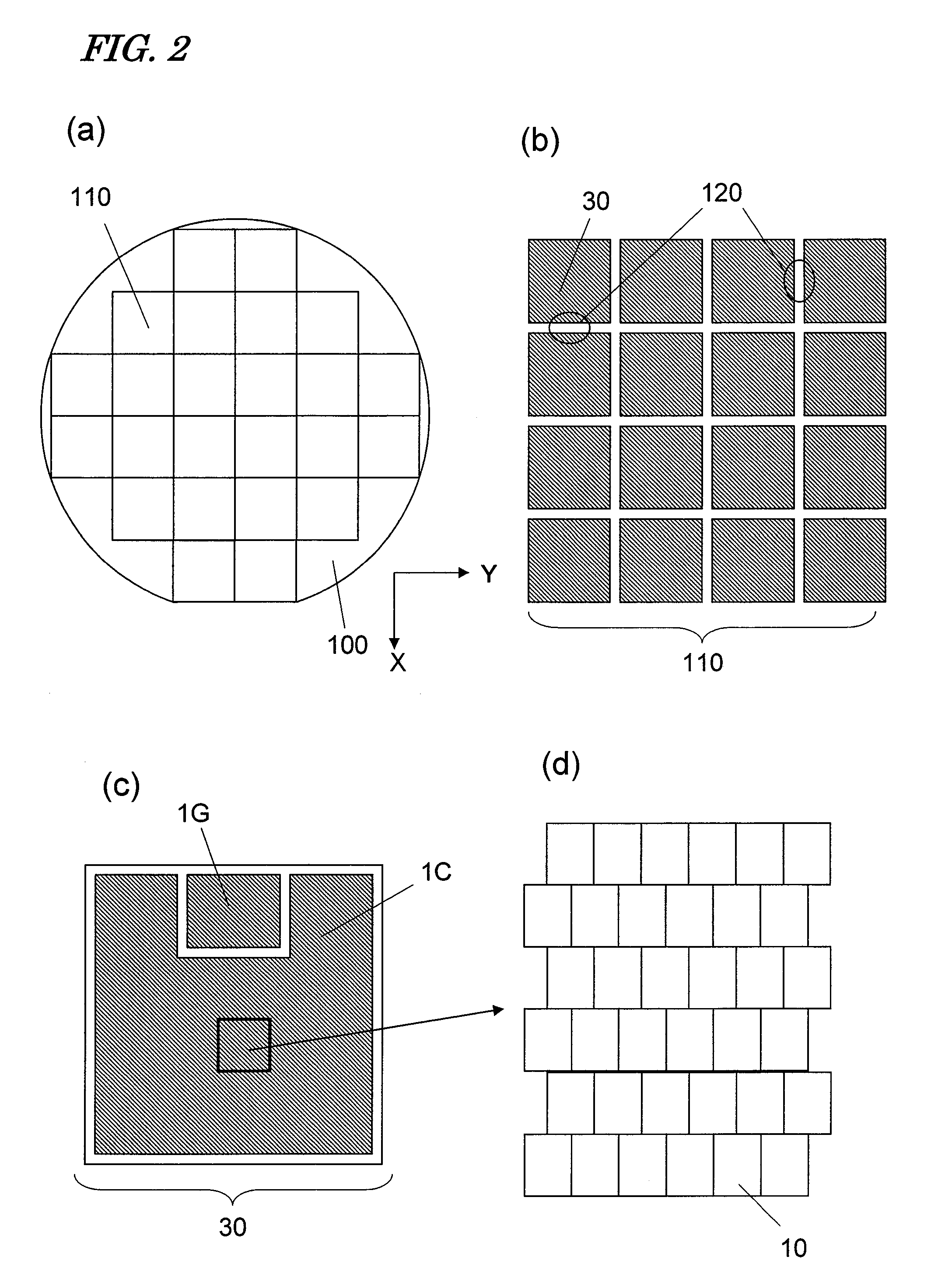
[0066]FIGS. 1(a) through 1(c) are schematic representations illustrating a unit cell of the semiconductor device of the first preferred embodiment. Specifically, FIG. 1(a) is a plan view illustrating a unit cell of the semiconductor device of this preferred embodiment, FIG. 1(b) is a cross-sectional view of the unit cell as viewed on the plane Ib-Ib′, and FIG. 1(b) is a cross-sectional view of the unit cell as viewed on the plane Ic-Ic′. On the other hand, FIGS. 2(a) through 2(d) are schematic representations illustrating the relation between a semiconductor substrate in the shape of a wafer (which will be...

embodiment 2

[0152]Hereinafter, a second specific preferred embodiment of a semiconductor device according to the present invention will be described with reference to the accompanying drawings.

[0153]FIGS. 7(a) through 7(c) are schematic representations illustrating a semiconductor device as a second preferred embodiment of the present invention. Specifically, FIG. 7(a) is a plan view illustrating a unit cell of the semiconductor device of this preferred embodiment, FIG. 7(b) is a cross-sectional view of the unit cell as viewed on the plane VIIb-VIIb′, and FIG. 7(c) is a cross-sectional view of the unit cell as viewed on the plane VIIc-VIIc′. The relation between the unit cell and the semiconductor bulk substrate of this preferred embodiment is just as what has already been described with reference to FIG. 2. It should be noted that the planes VIIb-VIIb′ and VIIc-VIIc′ are parallel to the X and Y directions, respectively, in the semiconductor bulk substrate 100 shown in FIG. 2(a).

[0154]The unit ...


PUM


Abstract

A semiconductor device is fabricated on an off-cut semiconductor substrate 11. Each unit cell 10 thereof includes: a first semiconductor layer 12 on the surface of the substrate 11; a second semiconductor layer 16 stacked on the first semiconductor layer 12 to have an opening 16e that exposes first and second conductive regions 15 and 14 at least partially; a first conductor 19 located inside the opening 16e of the second semiconductor layer 16 and having a conductive surface 19s that contacts with the first and second conductive regions 15 and 14; and a second conductor 17 arranged on the second semiconductor layer 16 and having an opening 18e corresponding to the opening 16s of the second semiconductor layer 16. In a plane that is defined parallel to the surface of the substrate 11, the absolute value of a difference between the respective lengths of the second semiconductor layer 16 and the second conductor 18 as measured in the off-cut direction is greater than the absolute value of their difference as measured perpendicularly to the off-cut direction.

Description

TECHNICAL FIELD[0001]The present invention relates to a semiconductor device and a semiconductor wafer.BACKGROUND ART[0002]Silicon carbide (SiC) is a high-hardness semiconductor material with a greater bandgap than silicon (Si), and has been used extensively in various types of semiconductor devices including power elements, hostile-environment elements, high temperature operating elements, and radio frequency elements. Among other things, the application of SiC to power elements such as switching elements and rectifiers has attracted a lot of attention. This is because a power element that uses SiC can significantly reduce the power loss compared to a Si power element.[0003]Among various power elements that use SiC, switching elements such as a MOSFET and a MESFET are known as typical ones. Such a switching element can switch between ON state in which drain current of several amperes (A) or more flows and OFF state in which the drain current becomes zero by changing the voltages ap...

Claims


Application Information

Patent Timeline
IPC IPC(8): H01L29/24H01L23/52H01L29/772
CPCH01L29/66068H01L29/812H01L29/7828H01L29/045H01L29/0696H01L29/1608H01L2924/0002H01L23/544H01L2223/54426H01L2223/5446H01L2924/00
Inventor UCHIDA, MASAOUTSUNOMIYA, KAZUYAHASHIMOTO, KOICHI
Owner PANASONIC CORP
Why Eureka
Try Eureka