Switchable element

a technology of switchable elements and elements, which is applied in the direction of digital storage, semiconductor devices, instruments, etc., can solve the problems of not being able to achieve high areal density and provide non-volatile and fast operation, and the flash is too slow for many embedded applications, and achieves fast operation and high areal density.

Inactive Publication Date: 2010-08-05
GLOBALFOUNDRIES INC
View PDF2 Cites 21 Cited by
  • Summary
  • Abstract
  • Description
  • Claims
  • Application Information

AI Technical Summary

Benefits of technology

[0008]In light of the above, it is desired to provide a switchable element capable of serving as memory and / or logic cell. Especially, the switchable element is desired to be non-volatile, and in addition make a high areal density and / or fast operation possible.

Problems solved by technology

None of these existing technologies can be integrated with high areal density and provide at the same time non-volatile and fast operation.
Especially, Flash is too slow for many embedded applications, SRAM and DRAM loose their memory state when disconnected from the power supply, and SRAM and MRAM can only be manufactured with a limited areal density.
In addition, the high programming voltage of Flash complicates integration with CMOS circuitry.
The always maintained input voltage will lead to considerable power consumption and heating in future CMOS generations.

Method used


Image

  • Switchable element
  • Switchable element
  • Switchable element

Examples


Embodiment Construction

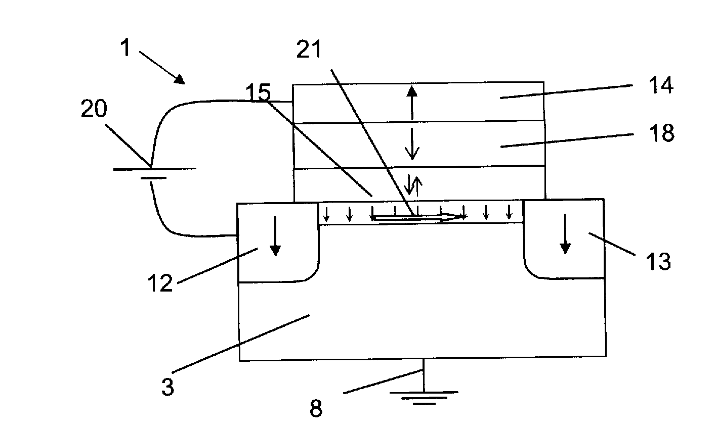
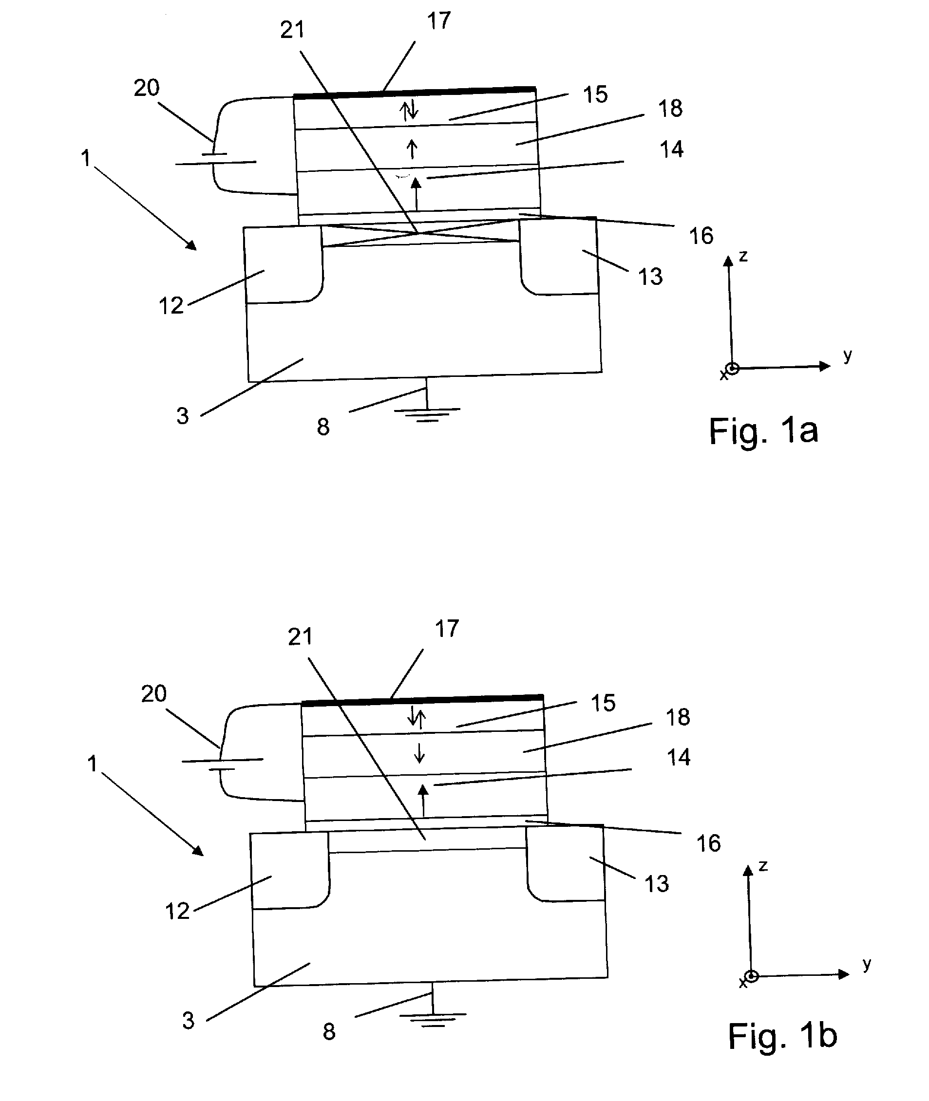
[0017]Ferroelectric materials possess a spontaneous polarization that is stable and can be switched hysteretically by an applied electric field. Ferromagnetic materials possess a spontaneous magnetization that is stable and can be switched by an applied magnetic field. Multiferroic materials possess simultaneous ferroelectric and magnetic ordering. These two order parameters are coupled. There exist ferromagnetic, ferrimagnetic, and antiferromagnetic multiferroics.

[0018]The multiferroic material is therefore programmable by application of an electrical signal, for example by the application of an electric field pulse, across it. Due to the coupling of the antiferromagnetic order parameter to the ferroelectric order parameter, this causes the antiferromagnetic order parameter to be programmed, too. By this, due to the exchange coupling of the antiferromagnet to the ferromagnetic material, the magnetization direction of the ferromagnetic material is also switched.

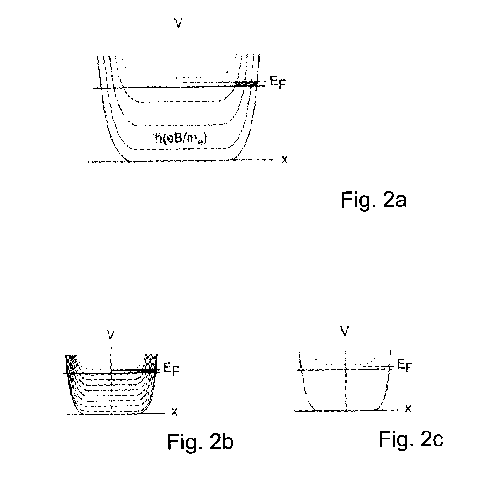
[0019]The multiferroi...


PUM


Abstract

A switchable element. The element includes a source electrode, a drain electrode, a conducting channel between the source electrode and the drain electrode, and a gate with multiferroic material being switchable, by application of an electrical signal to the gate, between a first switching state with a first spontaneous polarization direction and a second switching state with a second spontaneous polarization direction. The conducting channel is magnetoresistive, and a magnetic field strength at the conducting channel in the first switching state is different than a magnetic field strength in the second switching state, whereby a current-voltage characteristic of the conducting channel is dependent on the switching state of the multiferroic material.

Description

CROSS REFERENCE TO RELATED APPLICATION[0001]This application claims priority under 35 U.S.C. 119 from European Patent Application 09151813.4, filed Jan. 30, 2009,the entire contents of which are incorporated herein by reference.BACKGROUND OF THE INVENTION[0002]1. Field of the Invention[0003]The present invention is in the field of switchable elements and pertains to a switchable element, and to a memory device containing a plurality of such switchable elements as memory elements or a logic circuit containing such switchable elements as switchable logic elements.[0004]2. Description of Related Art[0005]Memory and logic elements such as complementary metal-oxide-semiconductor (CMOS) are major classes of integrated circuits. They are used in processor and / or memory chips such as microprocessors, microcontrollers, solid-state stand-alone and embedded memory circuits and other digital logic circuits.[0006]The most widely used memory technologies are DRAM, SRAM, Floating gate (Flash), and...

Claims


Application Information

Patent Timeline
Patent Type & Authority Applications(United States)
IPC IPC(8): G11C11/14H01L29/78
CPCG11C11/16G11C11/161G11C11/1675
Inventor KARG, SIEGFRIED F.MEIJER, GERHARD INGMAR
Owner GLOBALFOUNDRIES INC
Why Eureka
Try Eureka