
Eureka
For R&D, Eureka makes reading and utilizing patents & technical documents easy.
Eureka AIR
Designed for self-driven R&D workflows. Generate viable solutions, solve complex R&D challenges, empower your innovation with AI.

Eureka Materials
Designed for material experts only. Revolutionize your material R&D, from search, analyze, to developing new materials.

TechResearch
Generate reliable direction feasibility study reports for your R&D in just a few steps.

TechSeek
Discover and master advanced knowledge NOW. Basics, ideas, possibilities, all at once.

TechMind
As an expert in R&D Theories, TechMind can generates customized viable solutions instantly.

TechRisk
Analyze your overall solution with one click, know your potential R&D risks in advance.

TechMonitor
Get weekly tech updates, stay abreast of the latest tech innovations and key insights.
METHOD AND STRUCTURE FOR PMOS DEVICES WITH HIGH K METAL GATE INTEGRATION AND SiGe CHANNEL ENGINEERING
- Summary
- Abstract
- Description
- Claims
- Application Information
AI Technical Summary
Benefits of technology
Problems solved by technology
Method used
Image

Examples
first embodiment
[0042]The heating step that is employed in this embodiment of the invention is an annealing step that is performed at a temperature from 800° C. to 100° C., with a temperature from 900° C. to 950° C. being more preferred. Moreover, the heating step of the invention is performed in an oxidizing ambient which includes at least one oxygen-containing gas such as, for example, O2, NO, N2O, ozone and air. In some embodiments, the oxygen-containing ambient may be admixed with each other (e.g., an admixture of O2 and NO). Alternatively, the at least one oxygen-containing gas may be admixed with an inert gas including one of argon, helium, xenon, neon, krypton and nitrogen. Preferably, the heating step is performed in an oxidizing ambient that includes O2.
[0043]The heating step may be performed for a variable period of time that typically ranges from 10 minutes to 300 minutes, with a time period from 60 minutes to 120 minutes being more typical. The heating step may be performed at a single ...
second embodiment
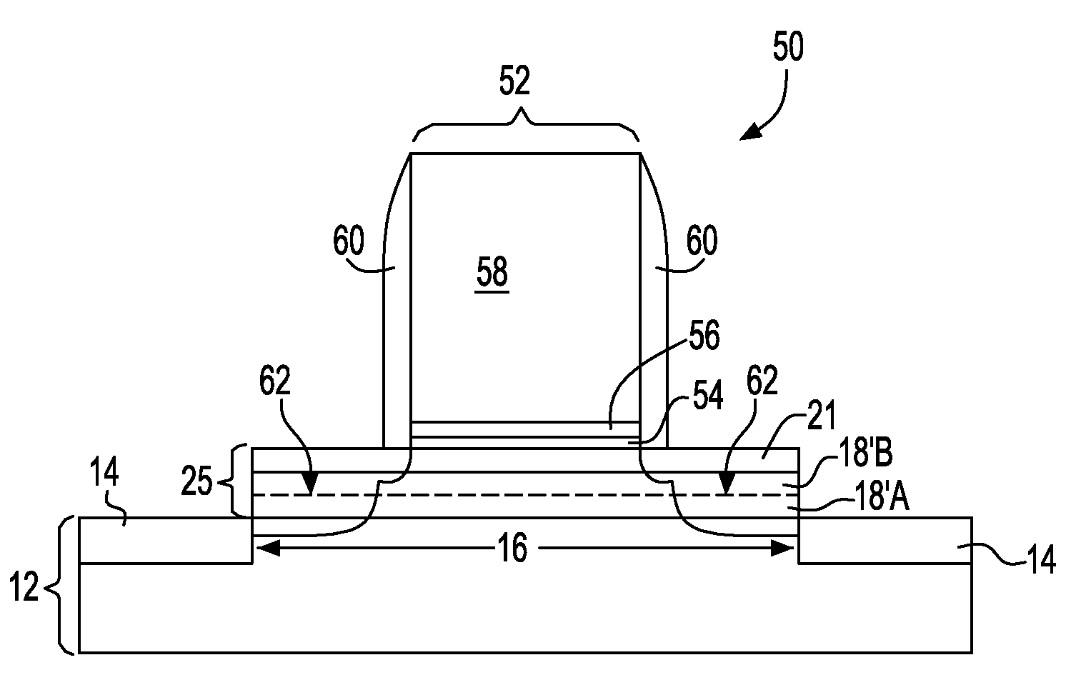
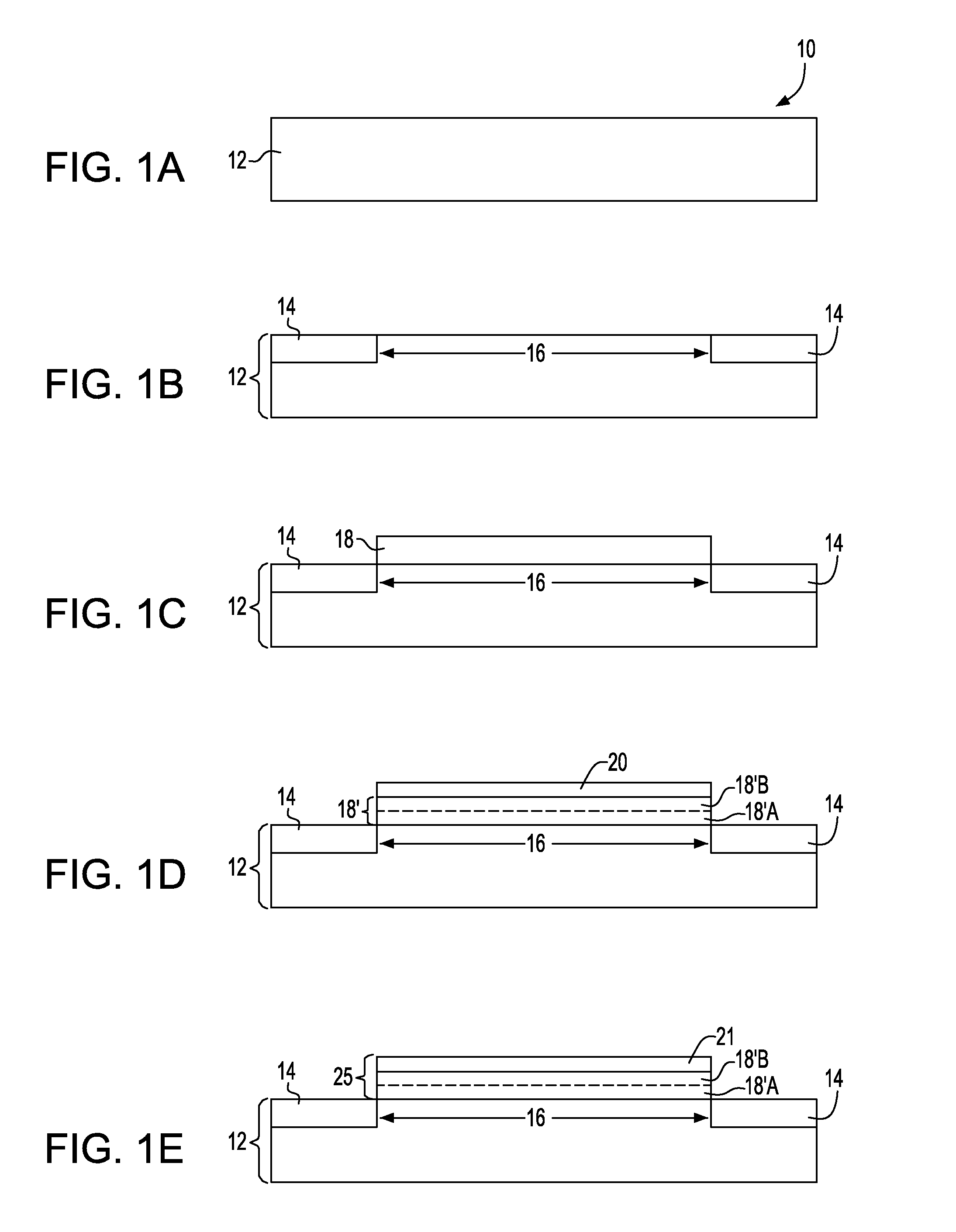
[0045]FIG. 1E illustrates the structure of FIG. 1D after stripping the surface oxide layer (e.g., oxide cap) 20 utilizing a conventional stripping process that is well known to those skilled in the art. Examples of stripping processes that can be employed to remove the surface oxide layer 20 include a wet etch using buffered hydrofluoric acid (HF) or dilute HF. A silicon cap 21 can now be grown on the oxidized and stripped SiGe layer 18′ to further protect the upper region 18′B of the SiGe film. The silicon cap 21 may be amorphous, polycrystalline, or single crystalline. The details of forming the silicon cap 21 are the same as that for forming silicon cap 22 of the invention. These details are provided below. The combination of the Si cap 21 and the oxidized and stripped SiGe layer 18′ forms a SiGe film 25 that includes a lower region (e.g., the oxidized and stripped SiGe layer including regions 18A′ and 18B′) that has a first Ge concentration and an upper region (e.g., the Si cap)...
third embodiment
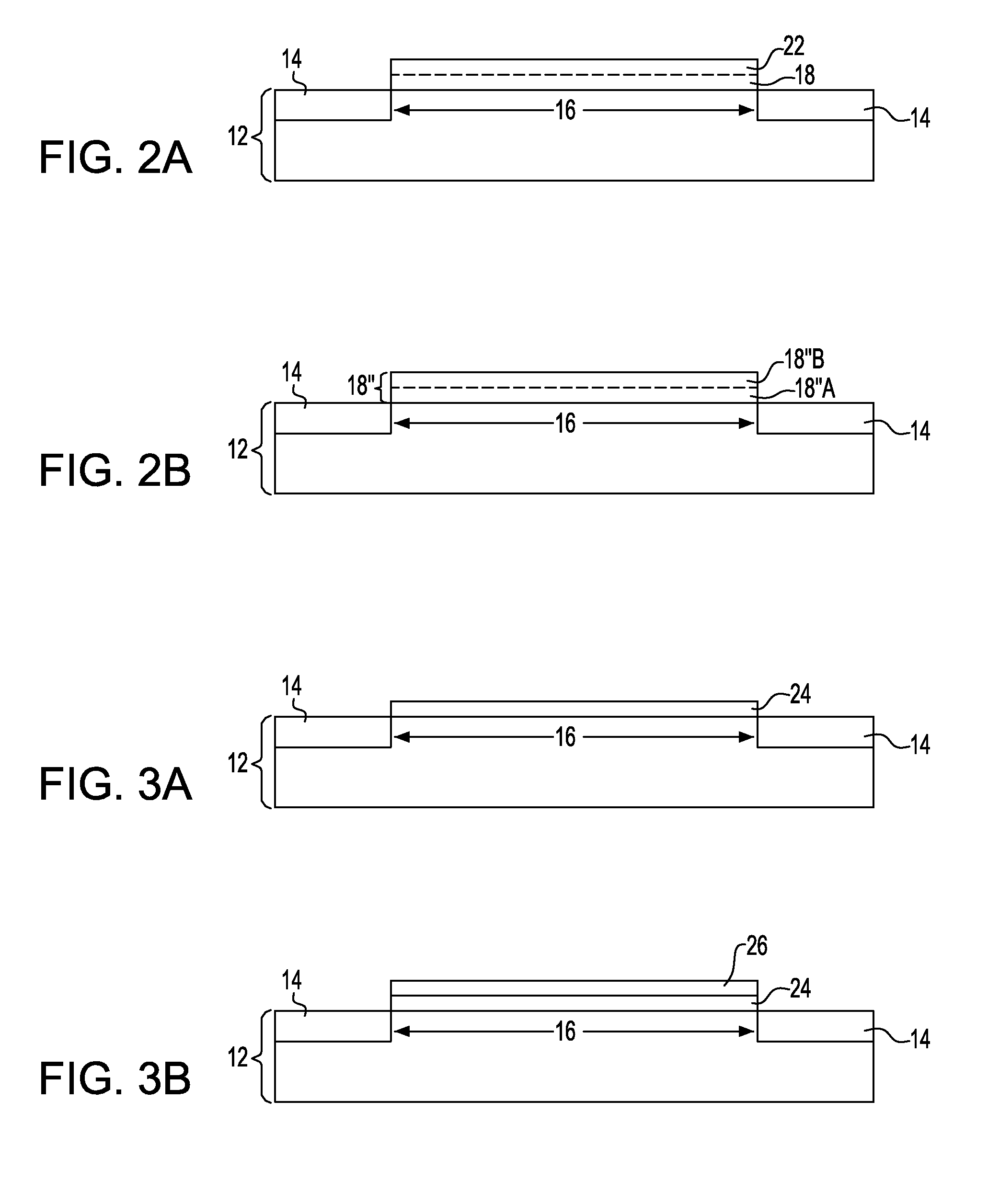
[0054]The SiGe layer 24 of the invention has a thickness from 20 angstroms to 100 angstroms, with a thickness from 50 angstroms to 80 angstroms being even more typical.
[0055]Next, and as shown in FIG. 3B, a SiGe cap 26 that has a lower Ge content than the SiGe layer 24 is formed utilizing conventional techniques well known to those skilled in the art including, for example, epitaxial growth, CVD, PECVD, ALD and chemical solution deposition. The Ge content of the SiGe cap 26 is about 25 atomic percent or less with a Ge content from 20 atomic percent to 25 atomic percent being even more typical. The SiGe cap 26 of the third embodiment of the invention has a thickness from 5 angstroms to 100 angstroms, with a thickness from 10 angstroms to 50 angstroms being even more typical.
[0056]In this embodiment of the invention, the SiGe layer 24 and the SiGe cap 26 form a SiGe film 18′″ having a lower region having a higher Ge content than the upper region.
[0057]Reference is now made to FIG. 4 w...
PUM
 Abstract
Description
Claims
Application Information
 - R&D Engineer
- R&D Manager
- IP Professional
- Industry Leading Data Capabilities
- Powerful AI technology
- Patent DNA Extraction
Browse by: Latest US Patents, China's latest patents, Technical Efficacy Thesaurus, Application Domain, Technology Topic, Popular Technical Reports.
© 2024 PatSnap. All rights reserved.Legal|Privacy policy|Modern Slavery Act Transparency Statement|Sitemap|About US| Contact US: help@patsnap.com