Semiconductor structure and method of fabricating the semiconductor structure

a semiconductor structure and semiconductor technology, applied in the direction of solid-state devices, basic electric elements, electric devices, etc., can solve the problems of not being able to achieve desired characteristics of p-channel fet, and the crystal plane has not been used in the conventional planar cmos device, so as to improve the mobility of the carrier

Active Publication Date: 2010-08-19
UNISANTIS ELECTRONICS SINGAPORE PTE LTD
View PDF17 Cites 82 Cited by
  • Summary
  • Abstract
  • Description
  • Claims
  • Application Information

AI Technical Summary

Benefits of technology

[0020]In contrast to a conventional planar CMOS technique in design and fabrication for a field-effect transistor (FET), the present invention provides an SGT CMOS device formed on a conventional substrate using various crystal planes in association with a channel type and a pillar shape of an FET, without a need for a complicated device fabrication process. Further, differently from a design technique of changing a surface orientation in each planar FET, the present invention is designed to change a surface orientation in each SGT to achieve improvement in carrier mobility. Thus, a plurality of SGTs having various crystal planes can be formed on a common substrate to achieve a plurality of different carrier mobilities so as to obtain desired performance.

Problems solved by technology

Thus, even if the N-channel FET exhibits excellent characteristics, the P-channel FET cannot have desired characteristics.
However, the (110) crystal plane has not been used in the conventional planar CMOS device, because the electron mobility deteriorates in the (110) crystal plane.

Method used


Image

  • Semiconductor structure and method of fabricating the semiconductor structure
  • Semiconductor structure and method of fabricating the semiconductor structure
  • Semiconductor structure and method of fabricating the semiconductor structure

Examples


Embodiment Construction

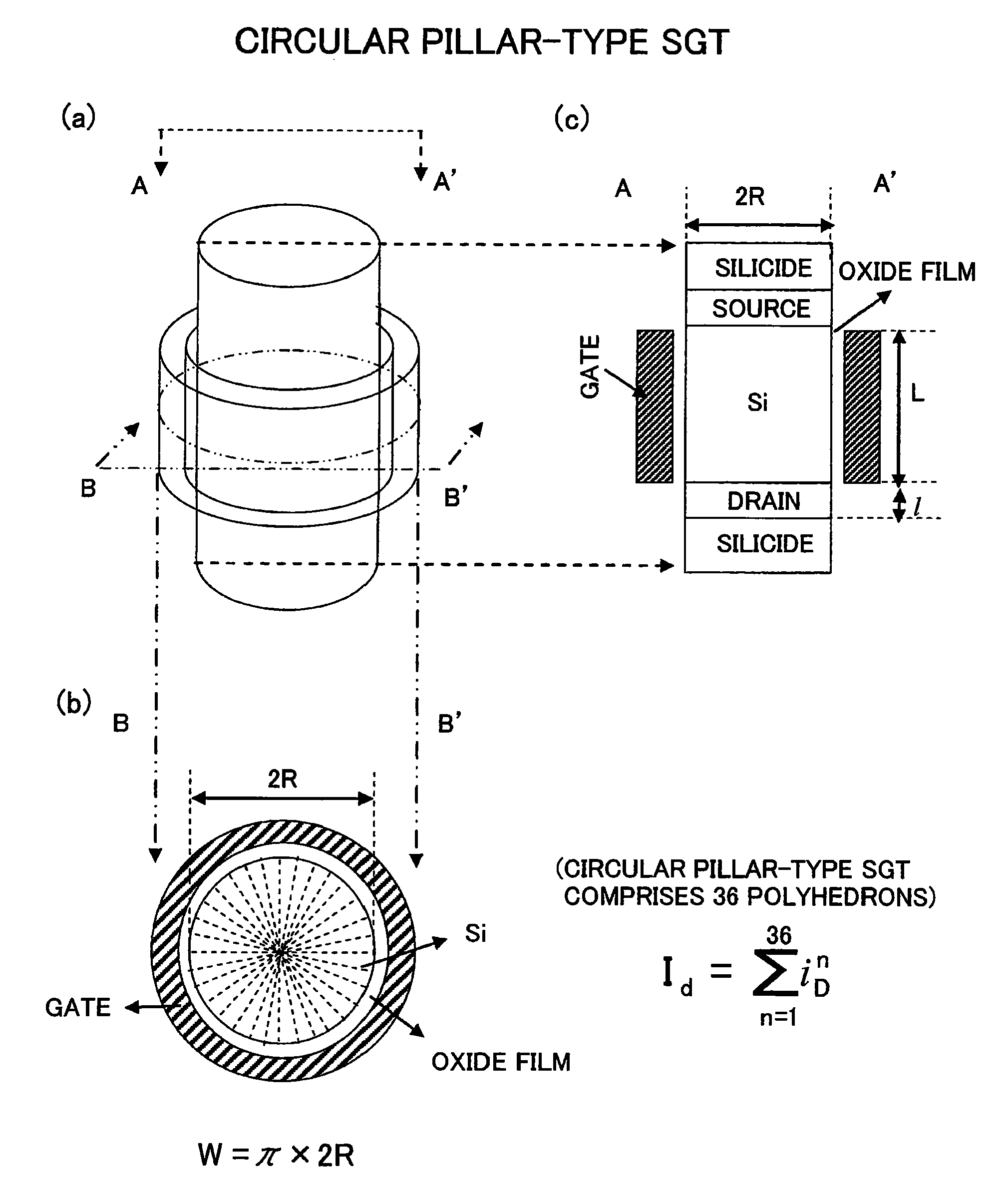
[0219]With reference to the accompanying drawings, the present invention will now be described based on various embodiments thereof. The same reference number is used for identifying the same constituent feature.

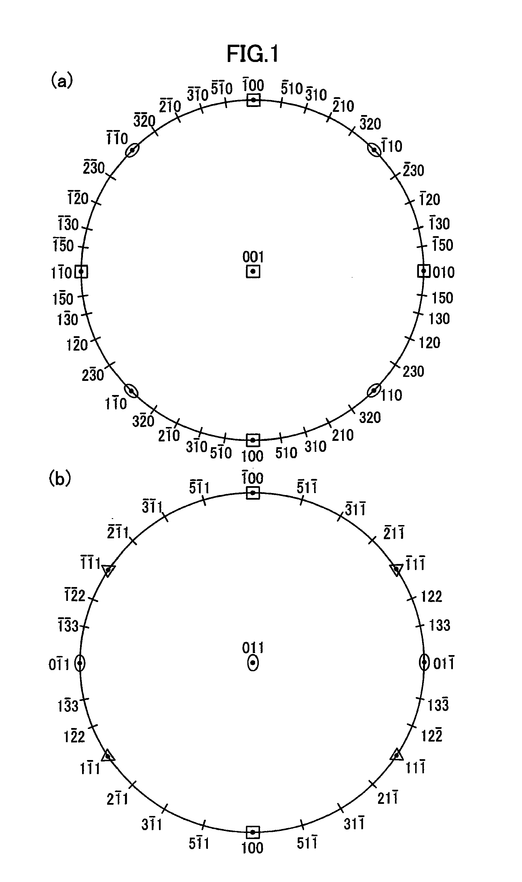
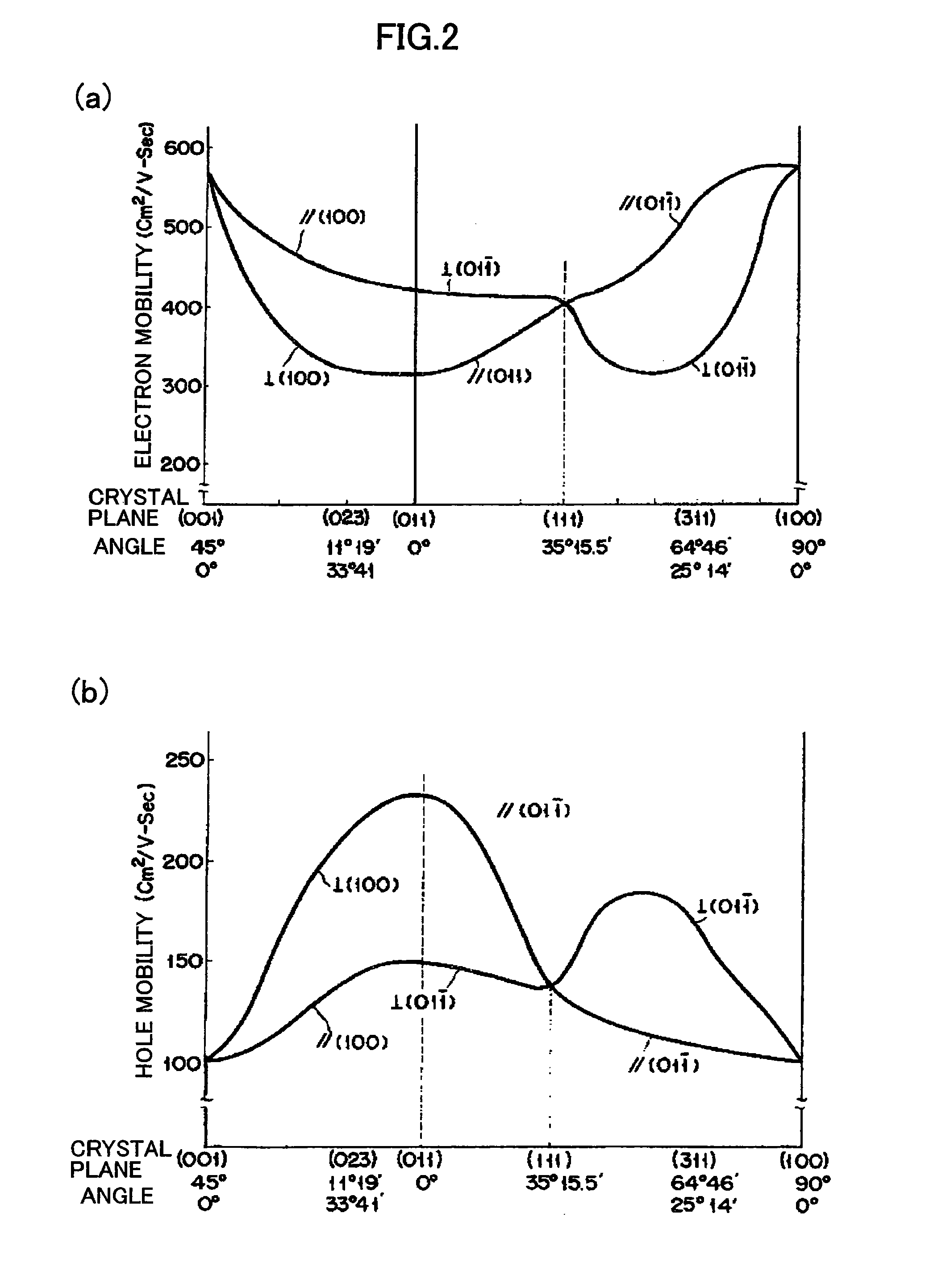
[0220]As mentioned above, in the present invention, various crystal planes are used for FET channels to optimize carrier mobility or reduce carrier mobility in each specific device element, based on physical properties of a semiconductor. For facilitating understanding of the present invention, an outline of crystal lattice and crystal orientation will be firstly described.

[0221]The present invention can be used in various methods for fabricating a plurality of CMOS SGTs on a common substrate using various crystal planes in association with a channel type and a pillar shape of an FET so as to optimize or reduce carrier mobility in each required specific device element to obtain desired performance. It will be understood by those skilled in the art that the present invention ...


PUM


Abstract

In contrast to a conventional planar CMOS technique in design and fabrication for a field-effect transistor (FET), the present invention provides an SGT CMOS device formed on a conventional substrate using various crystal planes in association with a channel type and a pillar shape of an FET, without a need for a complicated device fabrication process. Further, differently from a design technique of changing a surface orientation in each planar FET, the present invention is designed to change a surface orientation in each SGT to achieve improvement in carrier mobility. Thus, a plurality of SGTs having various crystal planes can be formed on a common substrate to achieve a plurality of different carrier mobilities so as to obtain desired performance.

Description

RELATED APPLICATIONS[0001]Pursuant to 35 U.S.C. §119(e), this application claims the benefit of the filing date of Provisional U.S. patent application Ser. No. 61 / 207,543 filed on Feb. 13, 2009. This application is a continuation application of PCT / JP2007 / 071052 filed on Oct. 29, 2007. The entire contents of these applications are hereby incorporated by reference.BACKGROUND OF THE INVENTION[0002]1. Field of the Invention[0003]The present invention relates to a semiconductor structure and a fabrication method for the semiconductor structure, pertaining primarily to an SGT CMOS technique.[0004]2. Description of the Background Art[0005]A CMOS (complementary metal-oxide semiconductor) technique, one of the elemental techniques for a very-large-scale integrated circuit (VLSI), is capable of forming literally tens of millions of transistors as a single integrated circuit. In the CMOS technique, there is a strong need for allowing ever-increasing device element density to be further increa...

Claims


Application Information

Patent Timeline
Patent Type & Authority Applications(United States)
IPC IPC(8): H01L29/78H01L21/20H01L29/04
CPCH01L21/823807H01L21/823828H01L21/823885H01L27/0922H01L29/78642H01L29/0657H01L29/42356H01L29/66666H01L29/7827H01L29/045
Inventor MASUOKA, FUJIOLEE, KEON JAE
Owner UNISANTIS ELECTRONICS SINGAPORE PTE LTD
Why Eureka
Try Eureka