

Solid-state image device and method of manufacturing the same
a solid-state image and image technology, applied in the field of solid-state image devices, can solve the problems of insufficient depth of photoelectric conversion regions and inability to accurately form impurity regions, etc., and achieve the effect of suppressing a reduction in sensitivity, high aspect ratio, and easy suppression of sensitivity
- Summary
- Abstract
- Description
- Claims
- Application Information
AI Technical Summary
Benefits of technology
Problems solved by technology
Method used
Image

Examples
first embodiment
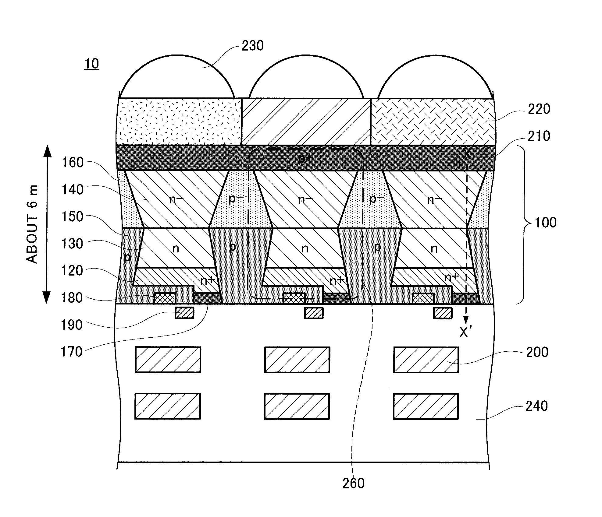
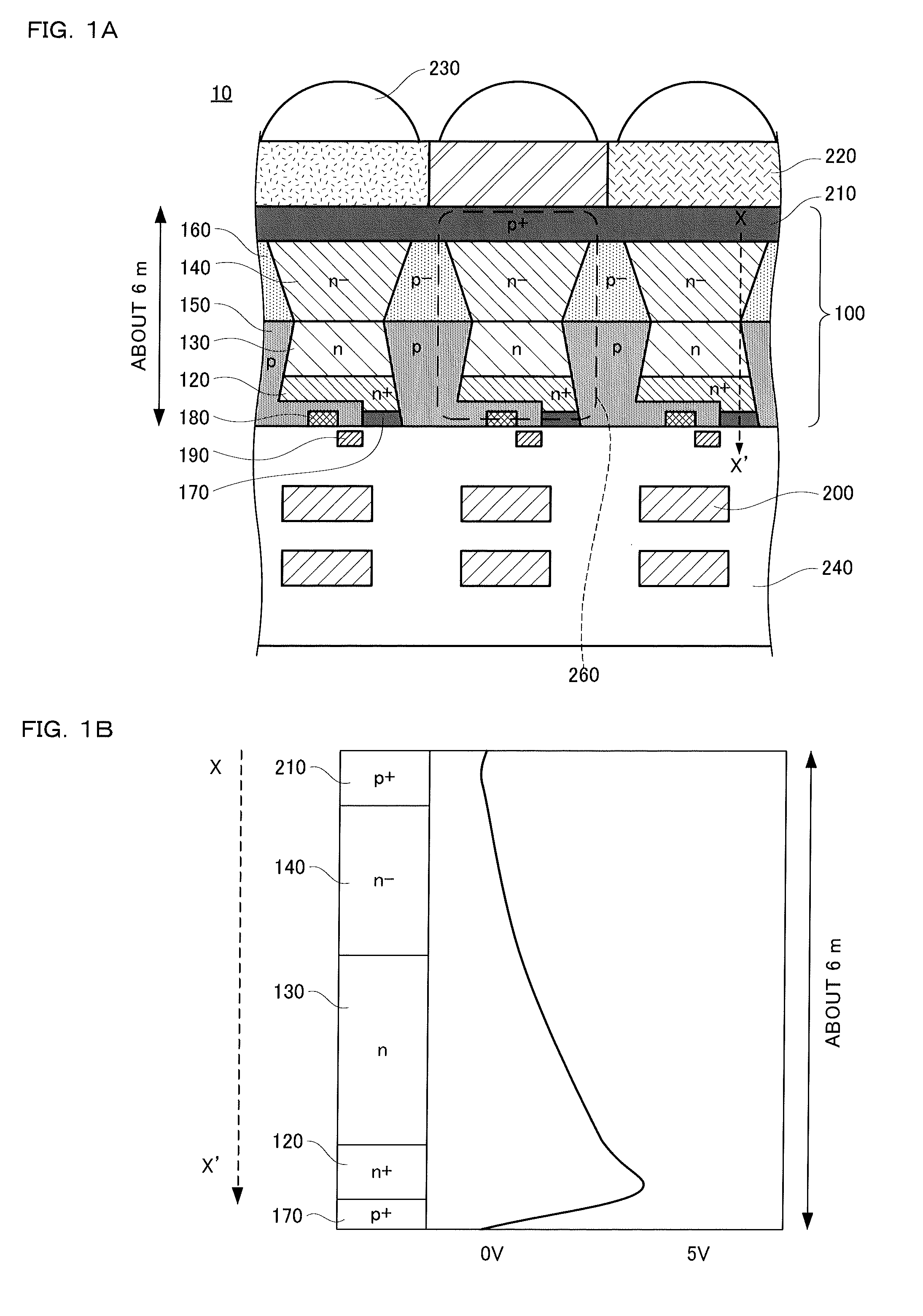
[0033]Referring to FIGS. 1A, 1B, and 2A to 2E, a solid-state image device and a method of manufacturing the same according to a first embodiment will be first described below.
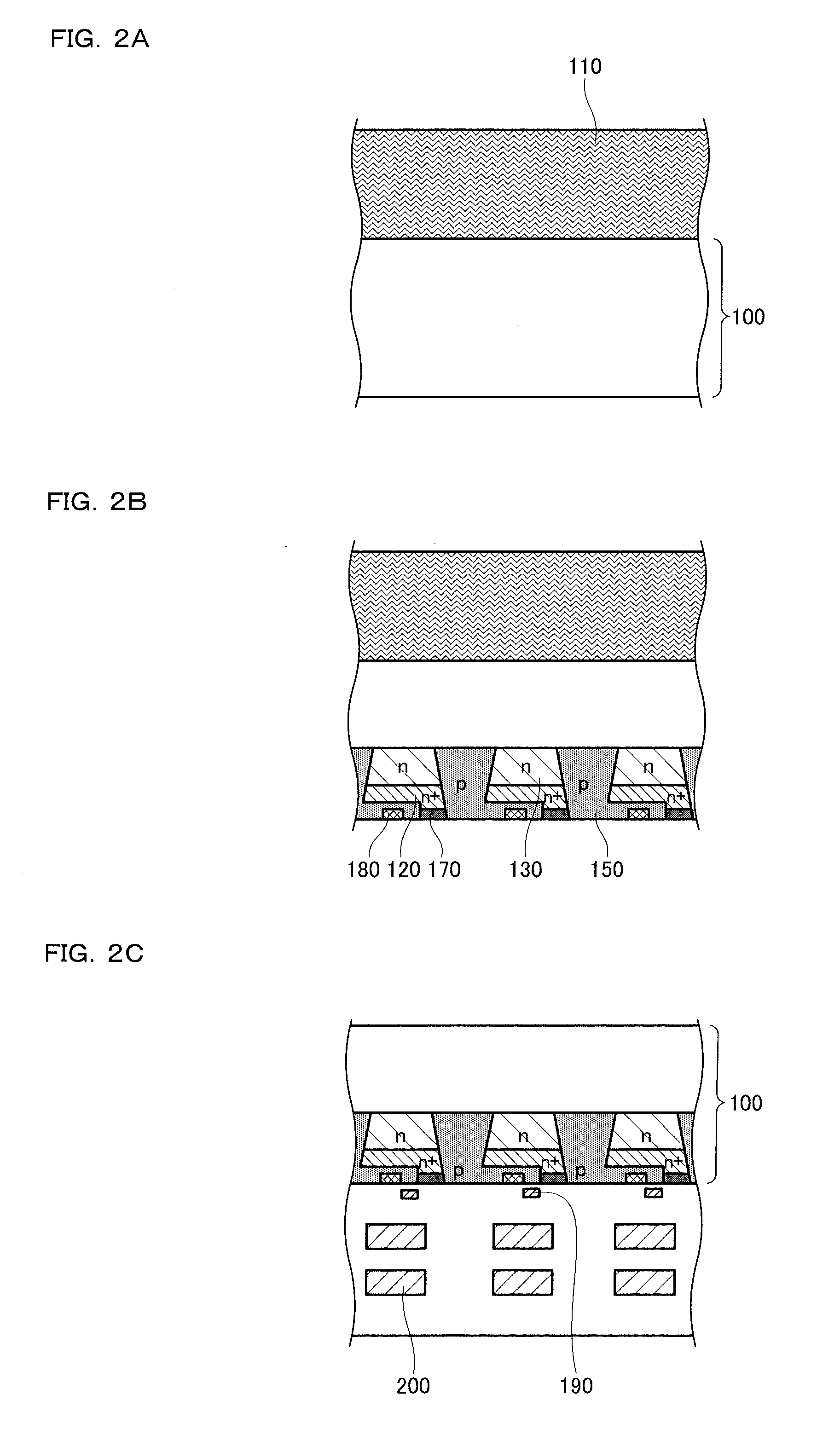
[0034]FIGS. 1A and 1B are explanatory drawings showing the solid-state image device according to the first embodiment. FIG. 1A is a sectional view showing the configuration of the solid-state image device according to the first embodiment and FIG. 1B shows a potential profile in cross section taken along line X-X′ of FIG. 1A. FIGS. 2A to 2E are process sectional views showing a method of manufacturing the solid-state image device of the present invention.
[0035]As shown in FIG. 1A, a backside-illumination solid-state image device 10 according to the first embodiment includes light receiving parts 260 formed in a p-type semiconductor substrate 100. The light receiving part 260 includes a charge storage region 120, a first n-type photoelectric conversion region 130 and a second n-type photoelectric conversion regi...
second embodiment
[0042]FIGS. 3A and 3B are explanatory drawings showing a solid-state image device according to a second embodiment. FIG. 3A is a sectional view showing the configuration of the solid-state image device according to the second embodiment and FIG. 3B shows a potential profile in cross section taken along line X-X′ of FIG. 3A.
[0043]As shown in FIG. 3A, a light receiving part 260 in a backside-illumination solid-state image device 30 of the second embodiment includes a first p-type semiconductor well 170 serving as a positive charge storage region, a charge storage region 120, a first n-type photoelectric conversion region 130, and a second n-type photoelectric conversion region 140. Further, the n-type impurity concentration of the second n-type photoelectric conversion region 140 is close to that of the first n-type photoelectric conversion region 130. The solid-state image device 30 of the second embodiment is different from the backside-illumination solid-state image device 10 of th...
third embodiment
[0045]FIGS. 4A and 4B are explanatory drawings showing a solid-state image device according to a third embodiment. FIG. 4A is a sectional view showing the configuration of the solid-state image device according to the third embodiment and FIG. 4B shows a potential profile in cross section taken along line X-X′ of FIG. 4A.
[0046]As shown in FIG. 4A, a light receiving part 260 in a solid-state image device 40 of the third embodiment includes a first p-type semiconductor well 170 serving as a positive charge storage region, a charge storage region 120, a first n-type photoelectric conversion region 130, and a second n-type photoelectric conversion region 140. Unlike the solid-state image devices of the first and second embodiments, a feature of the solid-state image device of the present embodiment is that a width W2 of the second n-type photoelectric conversion region 140 is larger than a width W1 of the first n-type photoelectric conversion region 130.
[0047]In this way, the second n-t...
PUM
 Abstract
Description
Claims
Application Information