Non-volatile semiconductor memory device

a semiconductor memory and non-volatile technology, applied in static storage, digital storage, instruments, etc., can solve the problems of erroneous reading, large the condition setting process requires a larger amount of time and cost, so as to reduce erroneous reading and reduce erroneous reading

Active Publication Date: 2010-08-19
RENESAS ELECTRONICS CORP
View PDF5 Cites 11 Cited by
  • Summary
  • Abstract
  • Description
  • Claims
  • Application Information

AI Technical Summary

Benefits of technology

[0012]Both of the first memory cell column and the first switch are formed by MONOS type transistors, whereby it is possible to provide the non-volatile semiconductor memory device with reduced erroneous reading.
[0013]According to the present invention, it is possible to provide the non-volatile semiconductor memory device with reduced erroneous reading.

Problems solved by technology

This condition setting process requires a larger amount of time and cost.
Thus, there is a problem that there is generated deviation in the timing of discharge in both sense terminals of the sense amplifier after the read target memory cell and the reference cell selection transistor are activated in the above reading operation, which may cause erroneous reading.

Method used


Image

  • Non-volatile semiconductor memory device
  • Non-volatile semiconductor memory device
  • Non-volatile semiconductor memory device

Examples


first exemplary embodiment

(First Exemplary Embodiment)

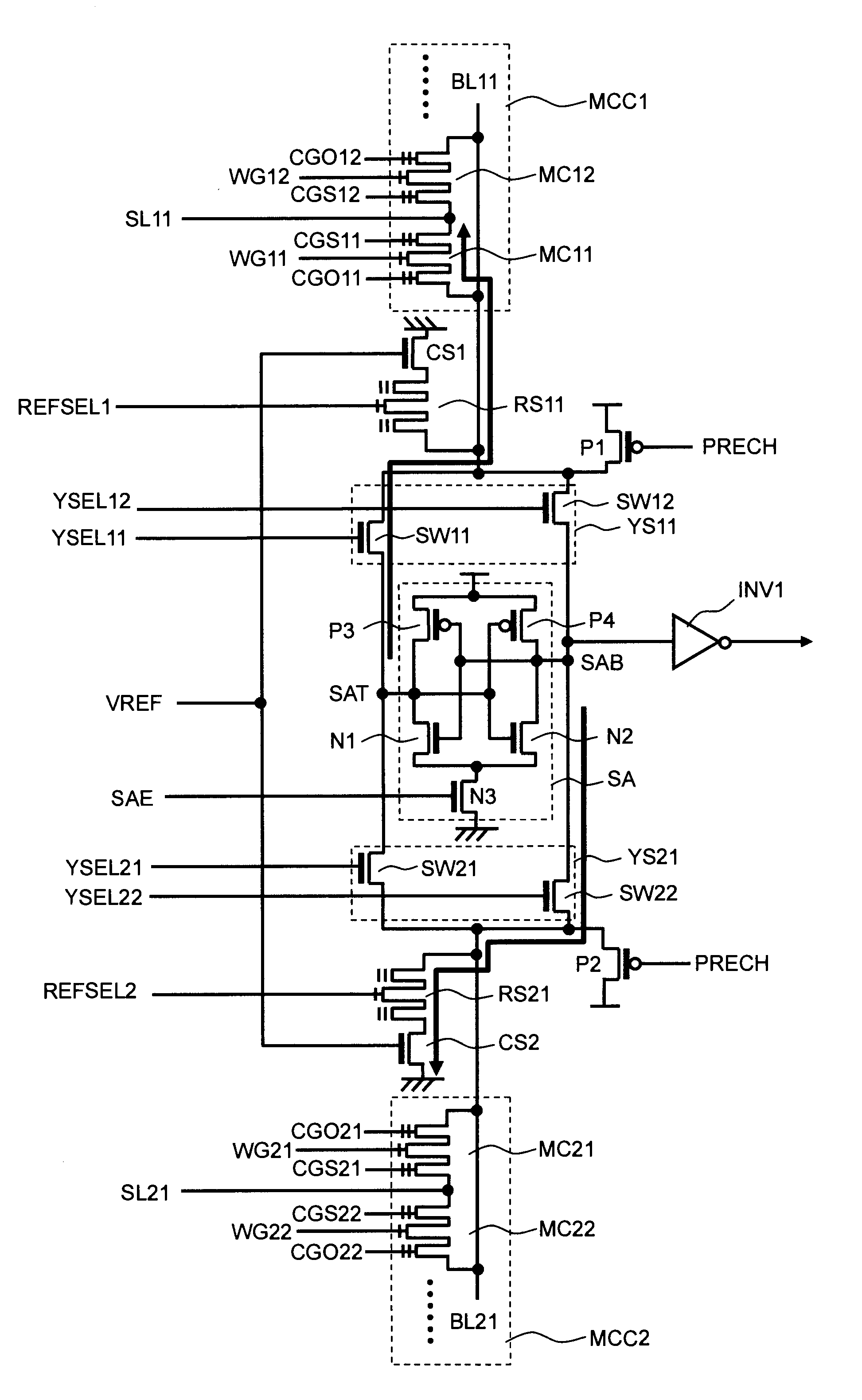
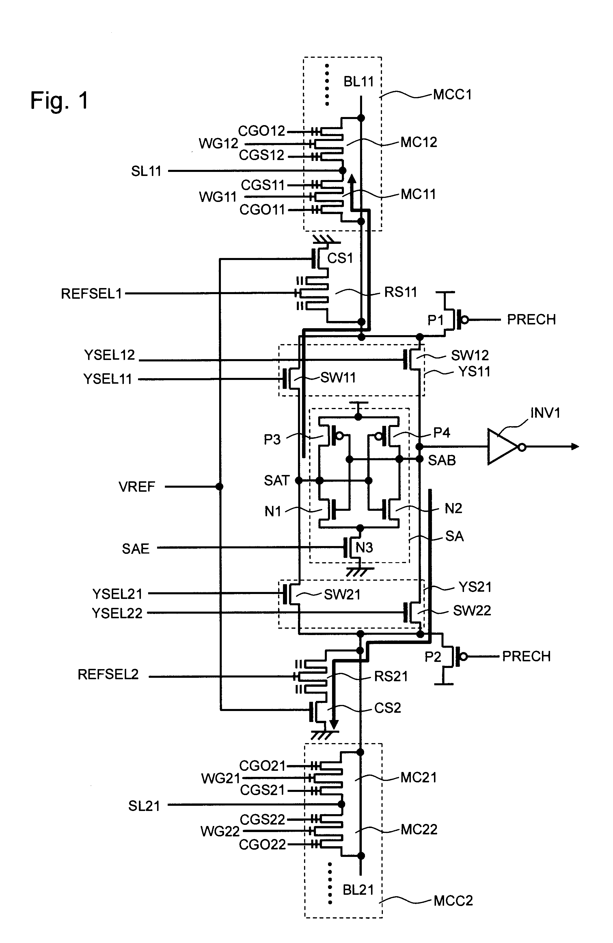
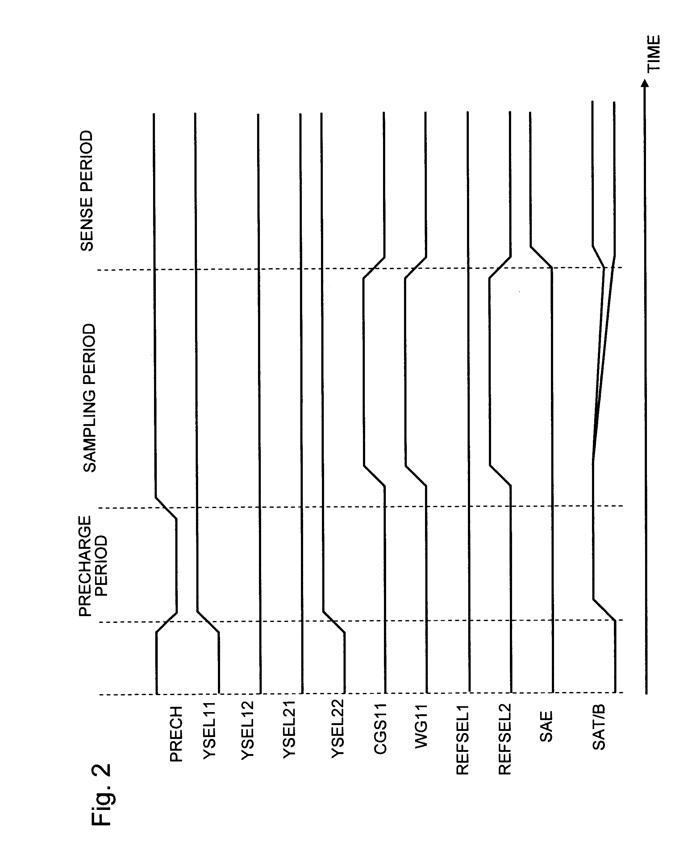
[0026]FIG. 1 is a circuit diagram of a non-volatile semiconductor memory device according to the first exemplary embodiment of the present invention. This non-volatile semiconductor memory device is a flash memory including a MONOS (Metal Oxide Nitride Oxide Semiconductor) transistor in each memory cell. This non-volatile semiconductor memory device includes a sense amplifier SA, an inverter INV1, a pair of Y selectors YS11, YS21, a pair of precharge transistors P1, P2, a pair of memory cell columns MCC1, MCC2, a pair of reference cell selection transistors RS11, RS21, and a pair of reference cells CS1, CS2. MONOS is also called SONOS (Silicon 1 Oxide Nitride Oxide Semiconductor). In this specification, the term MONOS is used to include both of them and collectively call the structure of a flash memory that includes a charge storage layer.

[0027]The sense amplifier SA is a latch type sense amplifier, and includes a pair of inverters. More specifically, one...

second exemplary embodiment

(Second Exemplary Embodiment)

[0060]Next, the second exemplary embodiment of the present invention will be described with reference to FIG. 7. FIG. 7 is a circuit diagram of a non-volatile semiconductor memory device according to the second exemplary embodiment. The circuit configuration of the non-volatile semiconductor memory device shown in FIG. 7 is different from that shown in FIG. 1 in that a plurality of bit lines are connected to each of the Y selectors YS11, YS21.

[0061]More specifically, n bit lines BL11 to BL1n are connected to the Y selector YS11. Here, the reference cell selection transistor RS11, and the memory cells MC11, MC12 are connected to the bit line BL11, as is similar to FIG. 1. Other bit lines BL12 to BL1n also have the same structures. Then, the reference cell selection transistor connected to each of the bit lines BL11 to BL1n is connected to the drain of the reference cell CS1 in common.

[0062]Further, n bit lines BL21 to BL2n are connected to the Y selector ...


PUM


Abstract

A non-volatile semiconductor memory device includes a sense amplifier, first and second bit lines that are connected to the sense amplifier, a first memory cell column that is connected to the first bit line, the first memory cell column being formed by a plurality of MONOS type transistors, a first constant current source that is connected to the second bit line, the first constant current source generating a reference current for the first memory cell column, and a first switch that is provided between the first constant current source and the second bit line, the first switch being formed by a MONOS type transistor.

Description

INCORPORATION BY REFERENCE[0001]This application is based upon and claims the benefit of priority from Japanese patent application No. 2009-033673, filed on Feb. 17, 2009, the disclosure of which is incorporated herein in its entirety by reference.BACKGROUND[0002]1. Field of the Invention[0003]The present invention relates to a non-volatile semiconductor memory device.[0004]2. Description of Related Art[0005]In a sense amplifier of a flash memory which is a non-volatile semiconductor memory device, as disclosed in Japanese Unexamined Patent Application Publication No. 2006-114154, for example, current from a target memory cell and current from a reference cell (reference current) are read out through the differential amplification. In this flash memory, a transistor having the same structure as the memory cell is used as a reference cell in order to reduce the influence of power supply voltage fluctuation.[0006]However, according to such a structure, it is needed to set the conditio...

Claims


Application Information

Patent Timeline
Patent Type & Authority Applications(United States)
IPC IPC(8): G11C16/06
CPCG11C16/28
Inventor HANYU, MASAMISUZUKI, JUNICHIYAMASHITA, JUNICHI
Owner RENESAS ELECTRONICS CORP
Why Eureka
Try Eureka