Wiring board and method of manufacturing the same

a technology of wiring board and manufacturing method, which is applied in the direction of semiconductor/solid-state device details, instruments, transportation and packaging, etc., can solve the problems of reduced production efficiency, low electrical resistance of feed-through electrodes, and difficult use of conductive pastes with considerably higher electrical resistance than those of copper plated layers, etc., to achieve high yield and production efficiency

Active Publication Date: 2010-08-26
SHINKO ELECTRIC IND CO LTD
View PDF7 Cites 11 Cited by
  • Summary
  • Abstract
  • Description
  • Claims
  • Application Information

AI Technical Summary

Benefits of technology

[0007]Exemplary embodiments of the present invention provide a wiring board in which a proper substrate strength can be obtained and a feed-through

Problems solved by technology

Thus, there is a problem in that a production efficiency is reduced.
When an electronic component having a high performance is to be mounted, however, a feed-through electrode having a low electrical resistance is required.
For this reason, it is hard to use a conductive paste having a considerably higher electrical resistance than that

Method used


Image

  • Wiring board and method of manufacturing the same
  • Wiring board and method of manufacturing the same
  • Wiring board and method of manufacturing the same

Examples


first embodiment

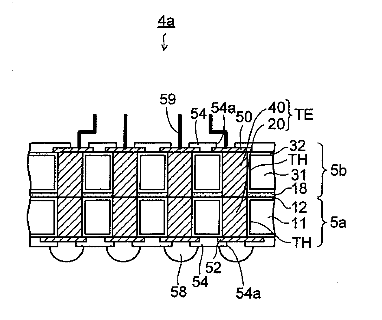
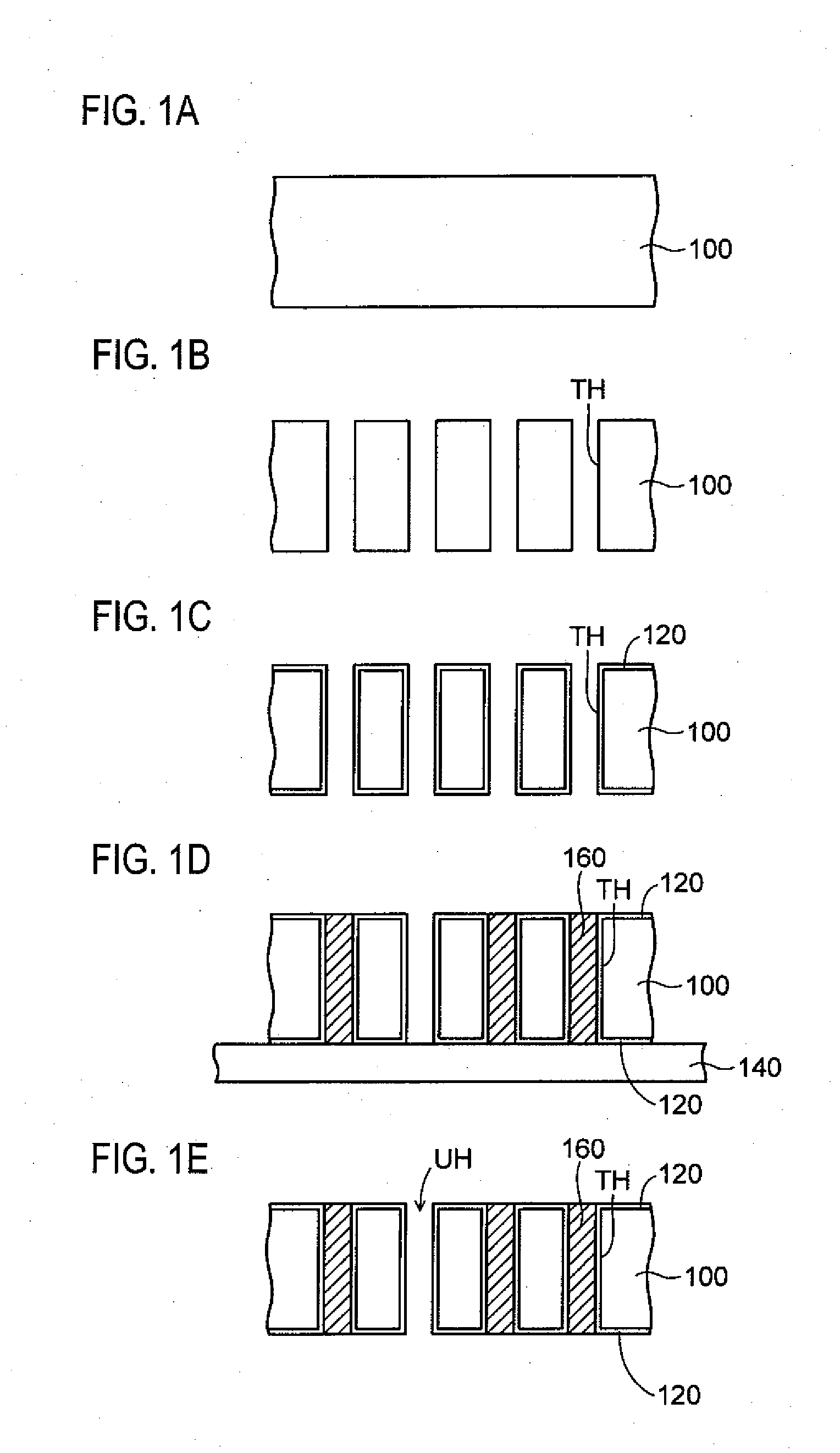
[0047]FIGS. 2A to 8C are sectional views showing a method of manufacturing a wiring board according to a first embodiment of the invention, FIG. 9 is a sectional view showing a wiring board according to a variant, FIG. 10 is a sectional view showing an electronic component device, and FIG. 11 is a sectional view showing a probe substrate.

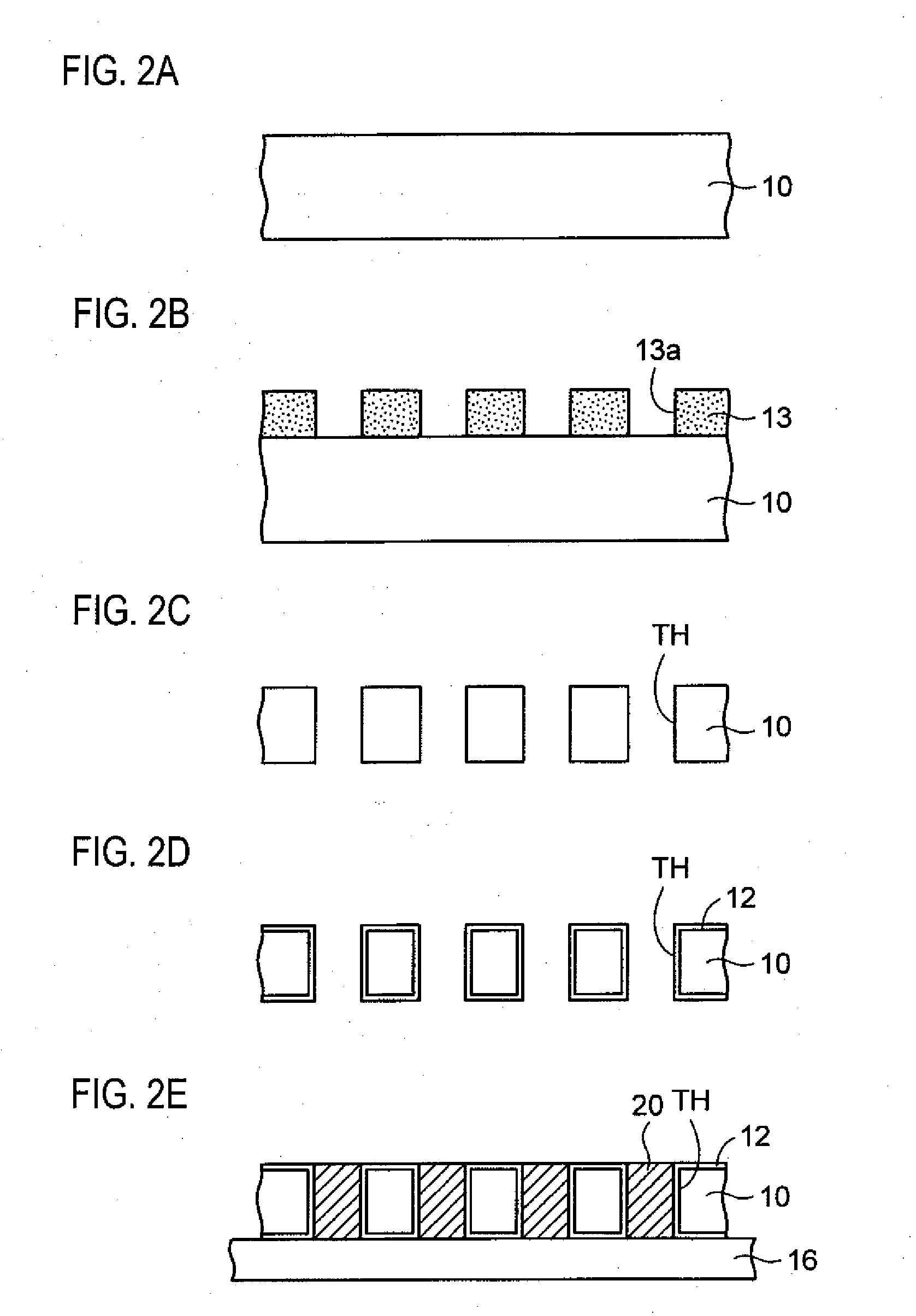
[0048]In the method of manufacturing a wiring board according to the first embodiment, as shown in FIG. 2A, a first silicon wafer 10 (a first wafer substrate) having a thickness of approximately 200 μm is first prepared. The first silicon wafer 10 is obtained by grinding a back face of a silicon wafer having a thickness of 725 μm by means of a grinder.

[0049]Although the first silicon wafer 10 having the thickness of approximately 200 μm which is thin is temporarily used in a process for manufacturing the wiring board in the embodiment, another second silicon wafer is stacked on the first silicon wafer 10 to additionally increase a substrate strength...

second embodiment

[0125]FIGS. 12A to 13C are sectional views showing a method of manufacturing a wiring board according to a second embodiment of the invention, FIG. 14 is a sectional view showing an electronic component device, and FIG. 15 is a sectional view showing a probe substrate.

[0126]The second embodiment is characterized in that a second silicon wafer is stacked on a first silicon wafer and a feed-through conductor portion is then formed in a through hole of the second silicon wafer. In the second embodiment, detailed description of the same steps as those in the first embodiment will be omitted.

[0127]Referring to the method of manufacturing a wiring board according to the second embodiment, as shown in FIG. 12A, the steps in FIGS. 2A to 2E according to the first embodiment are first executed to form a first feed-through conductor portion 20 in a through hole TH of a first silicon wafer 10 (a first wafer substrate). A thickness of the first silicon wafer 10 is approximately 200 μm in the sam...


PUM


Abstract

A wiring board includes a first substrate portion including a first feed-through conductor portion in a vertical direction, a second substrate portion provided on the first substrate portion and including a second feed-through conductor portion in a vertical direction of a corresponding part to the first feed-through conductor portion, and a feed-through electrode including the first feed-through conductor portion and the second feed-through conductor portion.

Description

[0001]This application claims priorities to Japanese Patent Application No. 2009-038932, filed Feb. 23, 2009, and Japanese Patent Application No. 2010-32040, filed Feb. 17, 2010, in the Japanese Patent Office. The Japanese Patent Application No. 2009-038932 and the Japanese Patent Application No. 2010-32040 are incorporated by reference in its entirety.TECHNICAL FIELD[0002]The present disclosure relates to a wiring board and a method of manufacturing the wiring board, and more particularly to a wiring board which can be applied to a mounting substrate for mounting an electronic component thereon or a probe substrate for evaluating an electrical characteristic of an electronic component, and a method of manufacturing the wiring board.RELATED ART[0003]There has been a multilayer wiring board including a feed-through electrode which is to be applied to a mounting substrate for mounting an electronic component thereon or a probe substrate for evaluating an electrical characteristic of a...

Claims


Application Information

Patent Timeline
IPC IPC(8): H05K1/11H05K13/00
CPCG01R1/07307Y10T428/24926H01L21/486H01L23/49827H05K3/423H05K3/4608H05K3/4647H05K2201/10674H05K2203/063H05K2203/0733H01L2224/16225H01L2224/32225H01L2224/73204H01L2924/15311G01R3/00Y10T29/49155Y10T428/24917H01L2924/00H01L2924/00014H01L2924/00011H01L2224/0401
Inventor SAKAGUCHI, HIDEAKISHIRAISHI, AKINORIHIGASHI, MITSUTOSHI
Owner SHINKO ELECTRIC IND CO LTD
Why Eureka
Try Eureka