System, apparatus, and method for pcb-based automation traceability

a technology of automation traceability and system, applied in the direction of inspection/indentification of circuits, burglar alarm mechanical actuation, instruments, etc., can solve the problems of affecting the efficiency of communication, and affecting the quality of communication, etc., to achieve the effect of improving communication efficiency

Active Publication Date: 2010-09-02
NXP BV
View PDF5 Cites 14 Cited by
  • Summary
  • Abstract
  • Description
  • Claims
  • Application Information

AI Technical Summary

Benefits of technology

[0008]The present invention utilizes already existing circuit traces or ground plane of a PCB. An embodiment of the present invention that uses the ground plane, splits the ground plane (making a dipole or folded dipole antenna) in a way that minimal ground plane needs to be removed therefore causing minimal impact to the operation of an end product containing the PCB, e.g., a cell phone, and takes advantage of the Frauhaufer zone, where communication is more efficient due to the electromagnetic as opposed to just magnetic fields.

Problems solved by technology

There are problems reading barcodes at different steps in an assembly process and bar codes can also become damaged or lost.
For example, instantaneous high temperatures are required to solder components to a PCB and PCB cleaning processes require acids, solvents and alkalis, all of which can damage conventional adhesive labels to a point where they fall off or become illegible.
This type of prior art PCB RFID take up additional costly area on the PCB.

Method used


Image

  • System, apparatus, and method for pcb-based automation traceability
  • System, apparatus, and method for pcb-based automation traceability
  • System, apparatus, and method for pcb-based automation traceability

Examples


Embodiment Construction

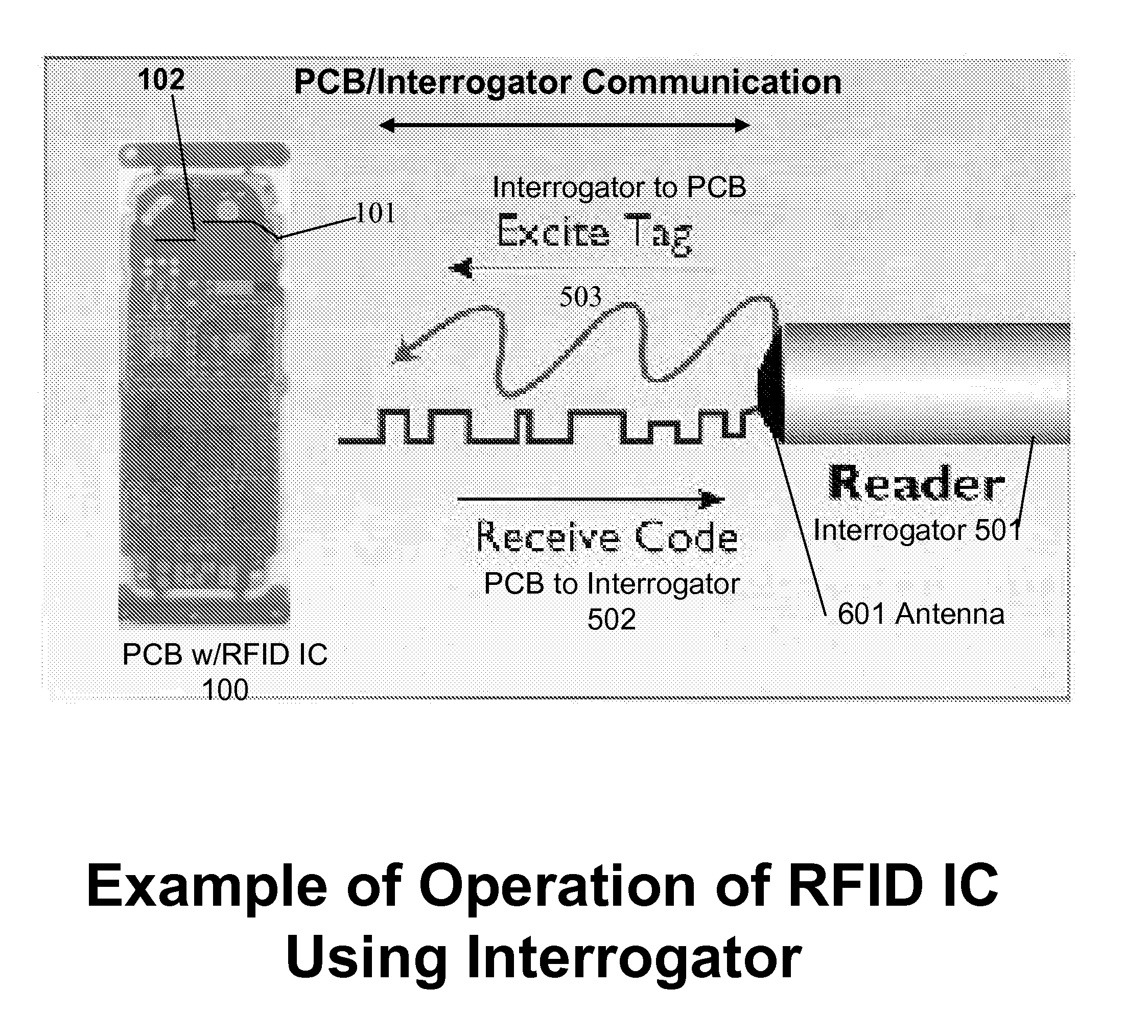
[0022]In the discussions which follow an assembly tracking process directed to a PCB is used as an example. Any end product requiring assembly process automation traceability and including a PCB according to the present invention can be tracked using the present invention.

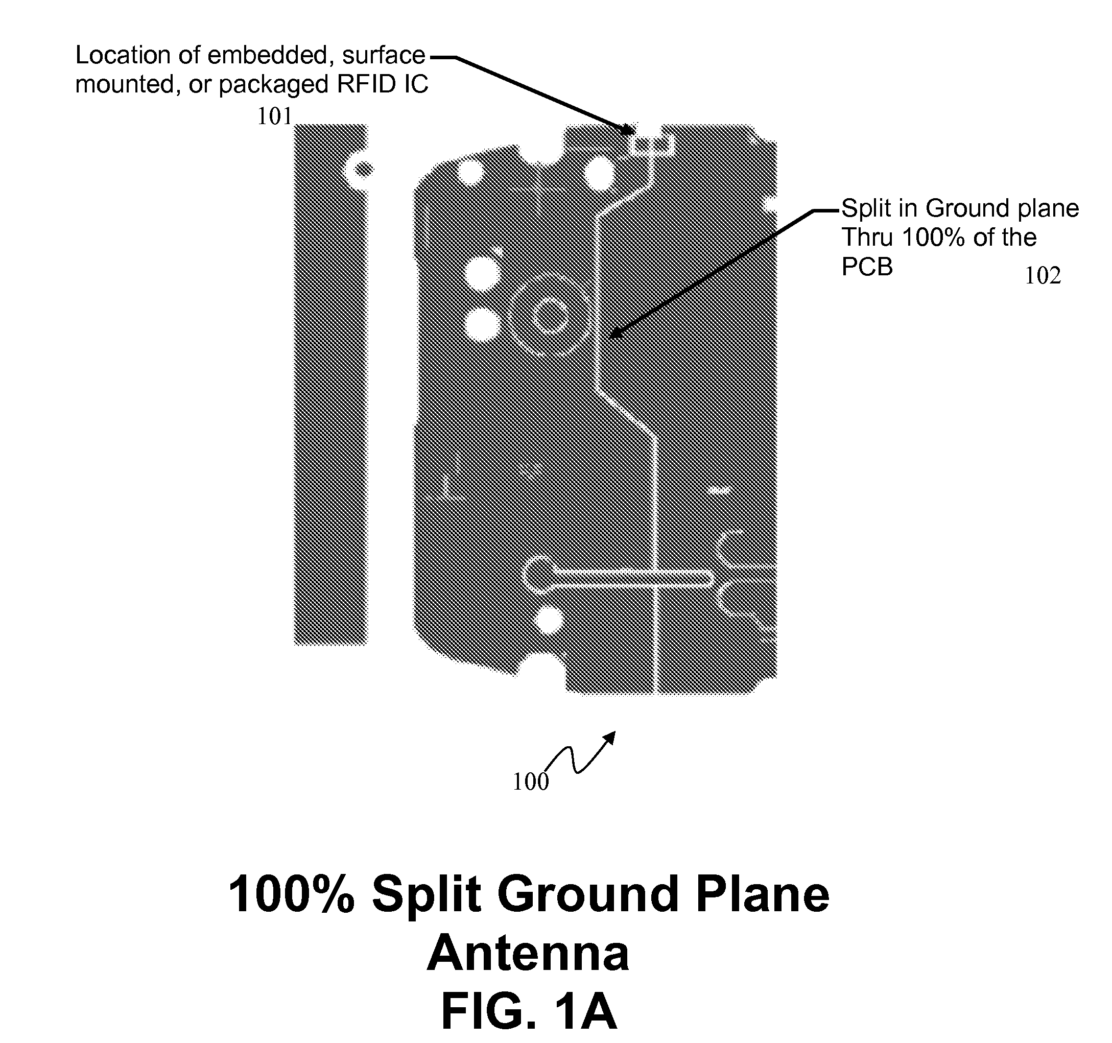
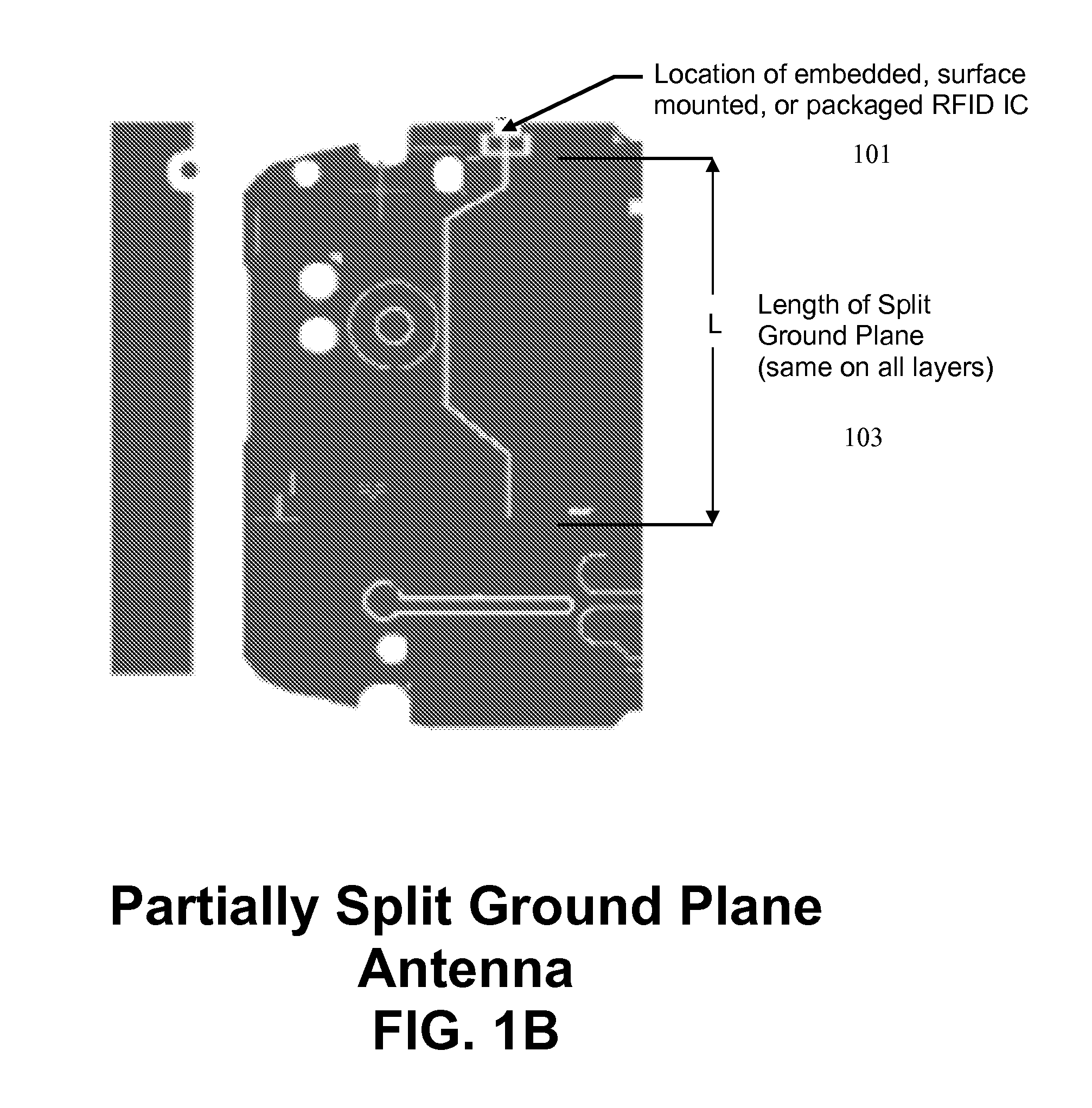
[0023]The present invention provides a system, apparatus, and method that use IC embedding technology to embed an RFID IC along with a dipole antenna within a PCB that in the example of a split ground plane antenna does not take up any additional area within the PCB. This configuration allows for a dipole structure that provides an adequate energy level received to power an RFID IC 101 circuit to the ‘on’ state therefore allowing RFID IC 101 / Electronic Product Code transactions. A die including the embedded RFID IC 101 has a low profile configuration which is essential in RFID labeling applications. A PCB or end product labeled with such an RFID IC 101, i.e., containing such an RFID IC 101, and including such an an...


PUM


Abstract

A system, apparatus, and method are provided for using a PCB component as an antenna to allow for RFID communication in the UHF band. The present invention enables supply chain management of a PCB and products containing the PCB by enabling tracking of a PCB at the assembly level such that at each production stage of the board production it is known exactly where the product is and what is its present state of test. One embodiment uses an existing ground plane of a PCB, splitting the ground plane of all the layers of the PCB, allowing for a dipole structure that provides an adequate received energy level to power the circuit to the “on” state thereby allowing RFID/Electronic Product Code transactions. In alternative embodiments, existing or added traces are used in place of the split ground plane as an antenna for the RFID IC. The supply chain management can employ a dedicated RFID interrogator that is connected to an IT network and allows for bill of materials to be fulfilled in an automated fashion throughout the assembly of the PCB. The manufacturer of the end product can also use the RFID IC in an own end product item level supply management system that includes inventory, shipments, and returns.

Description

CLAIM OF PRIORITY[0001]This application claims the benefit under 35 U.S.C. 119(a) of U.S. Provisional Application Ser. No. 60 / 857,748 entitled “CELL PHONE SPLIT GROUND PLANE RFID ANTENNA” filed in the United States Patent Office on Nov. 7, 2006, the entire contents of which are incorporated herein by reference.BACKGROUND OF THE INVENTION[0002]1. Field of the Invention[0003]The present invention relates to a system, apparatus, and method for using a cell phone ground plane as an antenna for an RFID IC die mounted on the surface of a PCB or embedded within the layers of a PCB attached to the antenna to form an RFID transponder. More particularly, the present invention relates to using existing or added traces, in addition to the split ground plane, as an antenna for the RFID IC. Most particularly, RFID supply chain management of PCBs and end products containing PCBs is enhanced by the present invention through use of the PCB, modified to include a transponder according to the present ...

Claims


Application Information

Patent Timeline
Patent Type & Authority Applications(United States)
IPC IPC(8): H04Q5/22
CPCG06K19/07749H01Q1/2225H01Q13/10H05K2201/10098H05K2201/093H05K2201/09663H05K1/0266
Inventor PAGANO, CHUCKKEENAN, RICHARD
Owner NXP BV
Why Eureka
Try Eureka