Scan signal line driver circuit and display device
a signal line and driver circuit technology, applied in the direction of digital storage, instruments, computing, etc., can solve the problems of display device such as a tft liquid crystal panel may suffer from such a display problem, and the level may change toward high, and achieve the effect of high resistance to nois
- Summary
- Abstract
- Description
- Claims
- Application Information
AI Technical Summary
Benefits of technology
Problems solved by technology
Method used
Image
Examples
embodiment 1
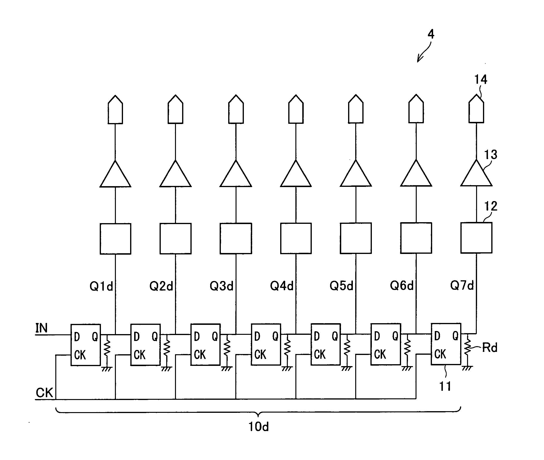
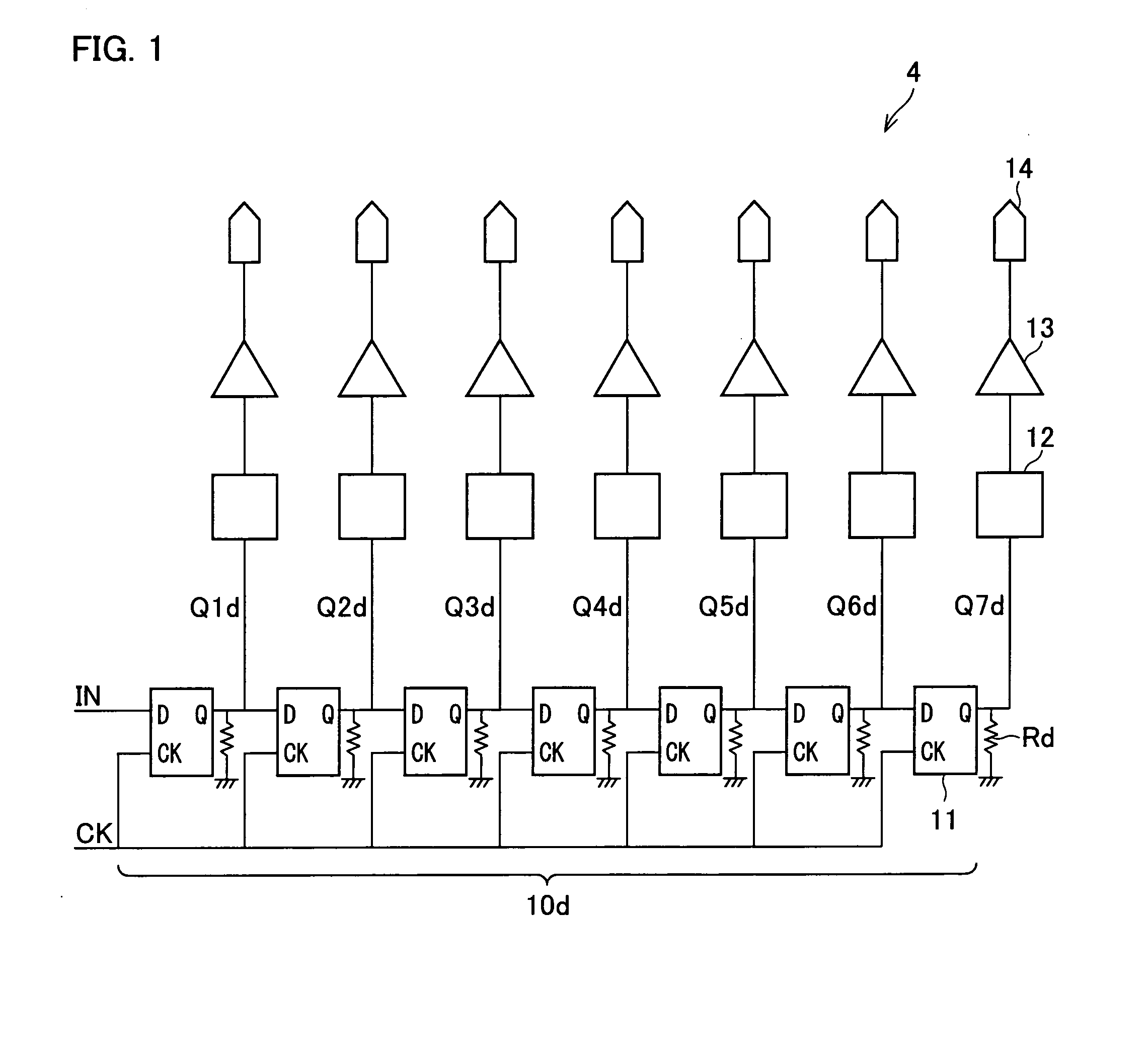
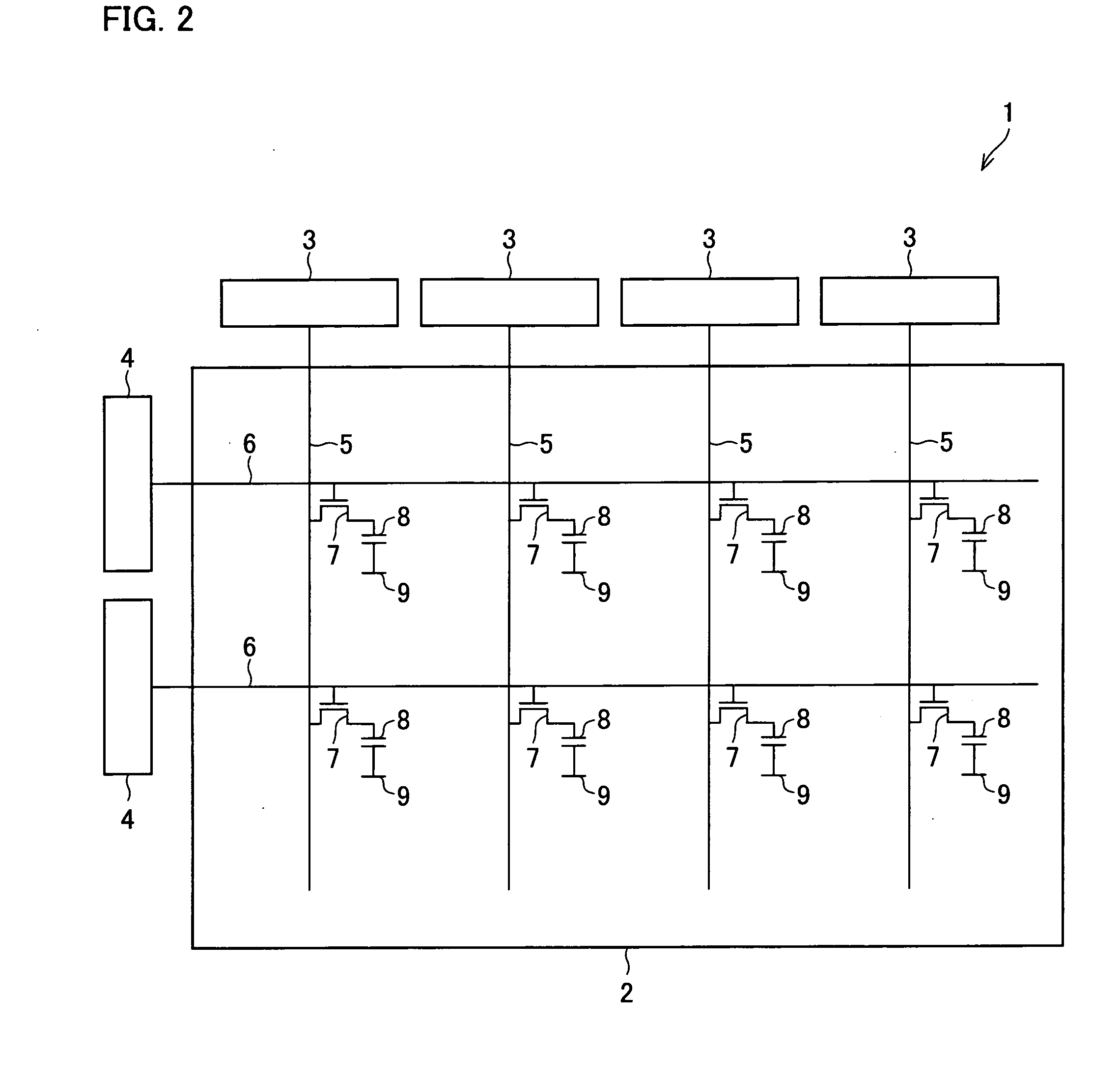
[0105]Embodiment 1 of the present invention is described below with reference to FIGS. 1 and 2.
[0106]FIG. 2 is a schematic view showing the configuration of a TFT liquid crystal panel 1 according to the present embodiment. The TFT liquid crystal panel 1 includes a glass substrate 2, source drivers 3, and gate drivers 4. The glass substrate 2 has source lines 5 and gate lines 6 provided thereon. Provided at each point of intersection between the source lines 5 and the gate lines 6 is a TFT 7 and a pixel 8 that has an end connected to a counter electrode 9. It should be noted here that the glass substrate 2, source drivers 3, source lines 5, gate lines 6, TFTs 7, pixels 8, and counter electrodes 9 of the TFT liquid crystal panel 1 are substantially identical to the glass substrate 102, source drivers 103, source lines 105, gate lines 106, TFTs 107, pixels 108, and counter electrodes 109 of the TFT liquid crystal panel 101 of FIG. 13, respectively, and as such, are not detailed below.
[...
embodiment 2
[0114]Embodiment 2 of the present invention is described below with reference to FIGS. 3 through 6. Although the gate drivers 4 according to Embodiment 1 have improved resistance to noise that causes a change in level toward High, the provision of the pull-down resistors Rd leads to degradation in resistance to noise that causes a change in level toward Low. In view of this, the present embodiment describes a configuration with improved resistance to noise that causes a change in level toward Low as well.
[0115]FIG. 3 is a circuit diagram showing the configuration of each gate driver 24 according to the present embodiment. Each gate driver 24 includes two shift registers 10d and 10u, seven level-shifter circuits 12, seven output buffers 13, seven output terminals 14, and seven OR circuits 15. That is, each gate driver 24 is configured by further providing the shift register 10u and the OR circuits 15 in such a gate driver 4 as shown in FIG. 1.
[0116]As with the shift register 10d, the...
embodiment 3
[0127]Embodiment 3 of the present invention is described below with reference to FIGS. 7 through 9. Embodiments and 2 have described a configuration having a pull-down or pull-up resistor provided between the data output terminal of each D-FF and the data input terminal of the next D-FF. This makes it possible to improve noise resistance between one D-FF and another; however, the influence of noise on the internal circuit of a D-FF may lead to a change in an output signal from the D-FF. In view of this, the present embodiment describes the configuration of a gate driver whose noise resistance has been improved by providing a pull-down resistor and a pull-up resistor inside of each D-FF.
[0128]FIG. 7 is a circuit diagram showing the configuration of each gate driver 34 according to the present embodiment. Each gate driver 34 is configured by replacing the shift registers 10d and 10u with shift registers 30d and 30u in such a gate driver 24 as shown in FIG. 3. The shift register 30d is...
PUM
 Abstract
Description
Claims
Application Information


