Photo Sensor With Pinned Photodiode and Sub-Linear Response

Inactive Publication Date: 2010-09-09
CSEM CENT SUISSE DELECTRONIQUE & DE MICROTECHNIQUE SA RECH & DEV
View PDF6 Cites 11 Cited by
  • Summary
  • Abstract
  • Description
  • Claims
  • Application Information

AI Technical Summary

Benefits of technology

[0011]As a consequence, it would be desirable to provide a photo sensor offering the advantages of a PPD over a conventional photodiode, but w

Problems solved by technology

Conventional photodiodes as employed in CMOS image sensors suffer from a set of practical limitations such as elevated dark current densities in excess of 1 nA/cm2, image lag seen as after-images of bright parts in a scene, photocharge transfer loss due to subthreshold ionization, as well as kTC or reset noise due to the inability to employ correlated multiple sampling techniques, as described for example by E. C. Fox et al., “A High Speed Linear CCD Image Sensor With Pinn

Method used


Image

  • Photo Sensor With Pinned Photodiode and Sub-Linear Response
  • Photo Sensor With Pinned Photodiode and Sub-Linear Response
  • Photo Sensor With Pinned Photodiode and Sub-Linear Response

Examples


Embodiment Construction

[0044]Definition: In a strict sense, a sub-linear function is a function whose second derivative is always negative (convex curve), while a super-linear function is a function whose second derivative is always positive (concave curve). In the present context, though, a device is considered to be sub-linear (or super-linear, respectively) if the second derivative of its voltage-current (current-voltage) characteristic is negative (positive) only over a substantial part of its operating range and zero elsewhere. However, a sub-linear (super-linear) behavior in the strict sense is advantageous.

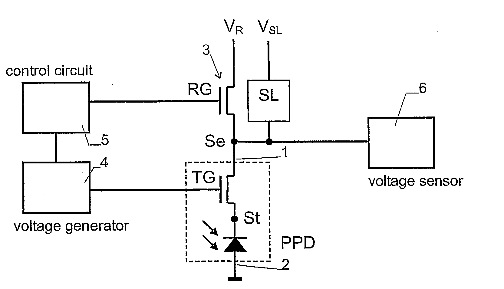
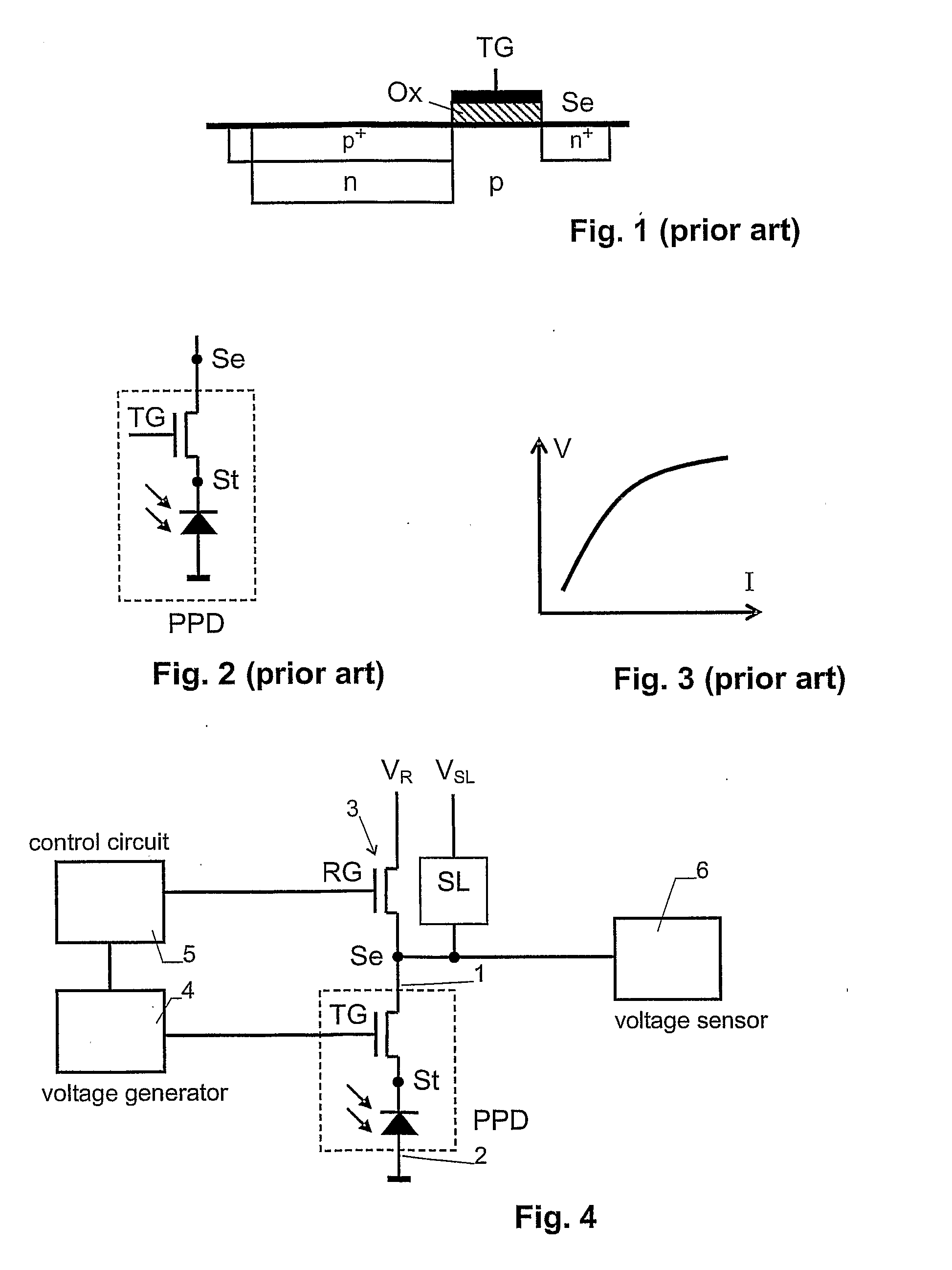
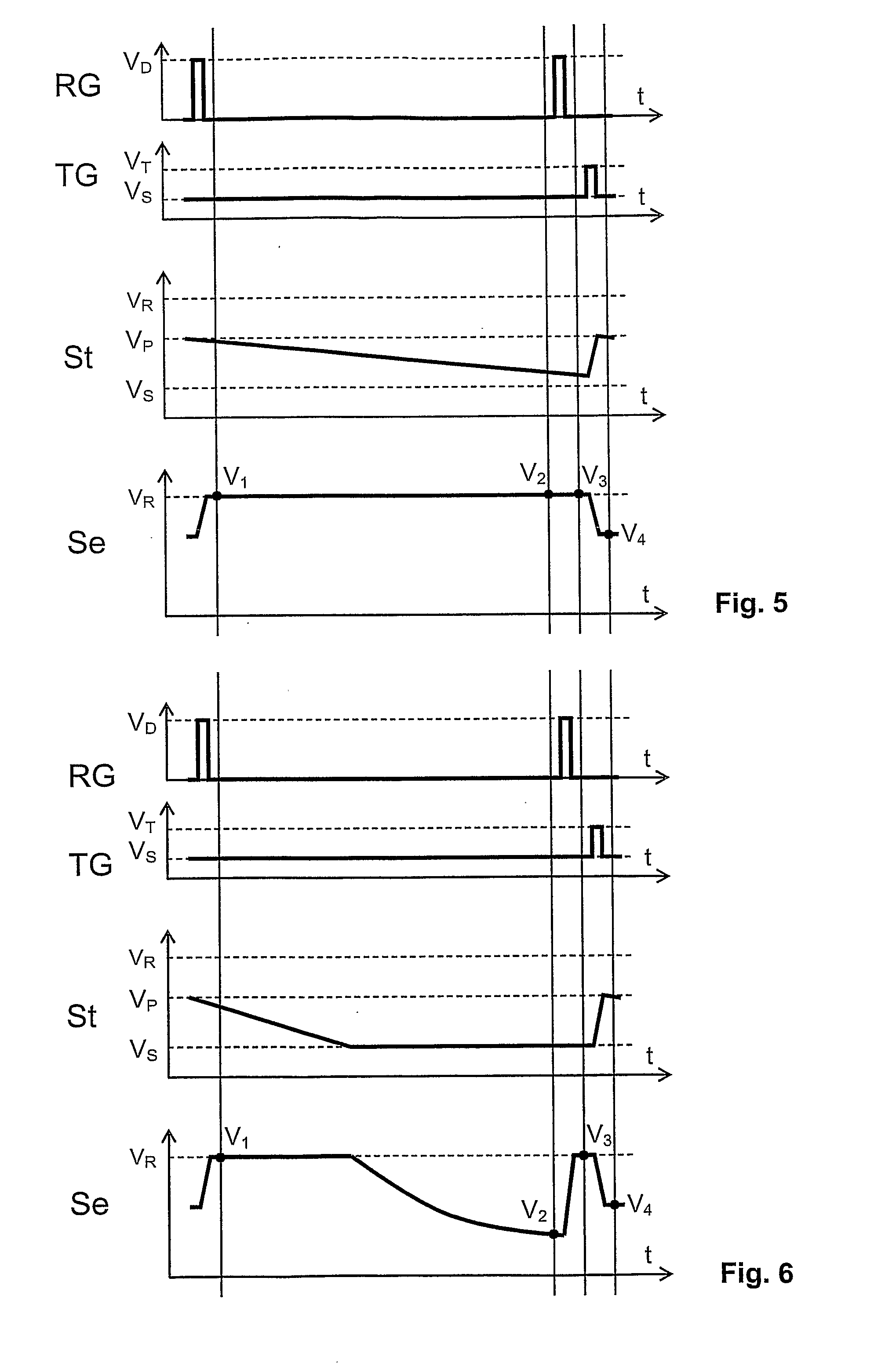
[0045]The basic operation of the photo sensor is illustrated by reference to FIGS. 4, 5 and 6.

[0046]As can be seen from FIG. 4, the photo sensor comprises a pinned photodiode PPD according to prior art having a first terminal 1 (photocharge sensing node), a second terminal 2 (anode) and a transfer gate TG. First terminal 1 is connected to the buried cathode of the PD through the transfer gate TG....


PUM


Abstract

A photo sensor exhibiting low noise, low smear, low dark current and high dynamic range consists of a pinned (or buried) photodiode (PPD) with associated transfer gate (TG), a reset circuit (3) and a device (SL) with sub-linear voltage-to-current characteristic. The exposure cycle is started by reverse biasing the buried photodiode to its pinning potential and by setting the transfer gate (TG) to a non-zero skimming potential. Photo-generated charge carriers start to fill the buried photodiode; if illumination intensity is high, excessive photocharges are flowing over the transfer gate (TG) to the sensing node. Because of the sub-linear device (SL) connected to the sensing node, the voltage at the sensing node is a sub-linear function of the illumination intensity, and hence the dynamic range of the pixel is increased. The voltage at the sensing node (Se) is read four times, namely before exposure, with the spilled-over photocharge, after reset, and after the photocharge in the buried photodiode has been transferred to the sensing node. This allows correlated multiple sampling techniques to be employed for eliminating reset noise. Because of its compact size, the photo sensor can be employed in one- and two-dimensional image sensors fabricated with industry-standard CMOS or CCD technologies.

Description

FIELD OF THE INVENTION[0001]The present invention relates to solid-state photo sensors for low-noise, low-smear, low-dark-current, one-dimensional and two-dimensional image sensing, where it is necessary to increase the dynamic range. In particular, the invention relates to a photo sensor and method for operating a photo sensor having a pinned photodiode (PPD) and sub-linear response.[0002]Further, the invention relates to CMOS (Complementary Metal Oxide Semiconductor) image sensors and to CCD (Charge Coupled Device) image sensors whose photosensitive devices consist of PPDs, and for which a higher dynamic range is desired than is possible with the known PPD device structures and operation.BACKGROUND[0003]Conventional photodiodes as employed in CMOS image sensors suffer from a set of practical limitations such as elevated dark current densities in excess of 1 nA / cm2, image lag seen as after-images of bright parts in a scene, photocharge transfer loss due to subthreshold ionization, ...

Claims


Application Information

Patent Timeline
IPC IPC(8): H01L31/103
CPCH04N3/155H04N25/573
Inventor SEITZ, PETERLUSTENBERGER, FELIX
Owner CSEM CENT SUISSE DELECTRONIQUE & DE MICROTECHNIQUE SA RECH & DEV
Why Eureka
Try Eureka