Flat display panel

Inactive Publication Date: 2010-09-09
AU OPTRONICS CORP
View PDF17 Cites 44 Cited by
  • Summary
  • Abstract
  • Description
  • Claims
  • Application Information

AI Technical Summary

Benefits of technology

[0009]Since the driving chip of the flat display panel of the present invention has the pins and the pitches of the pins are nonequivalent, the short circuit problem may be efficiently avoided due to the too small pitches in the prior art. Meanwhile, the conductive lines in the border portion electrically connected to the pins having larger pitches therebetwee

Problems solved by technology

Consequently, the pitches of the pins of chips have gradually become smaller, such that lots of technical problems are caused due to the scaled-down manufacturing process.
For instance, if the pitches

Method used


Image

  • Flat display panel
  • Flat display panel
  • Flat display panel

Examples


first embodiment

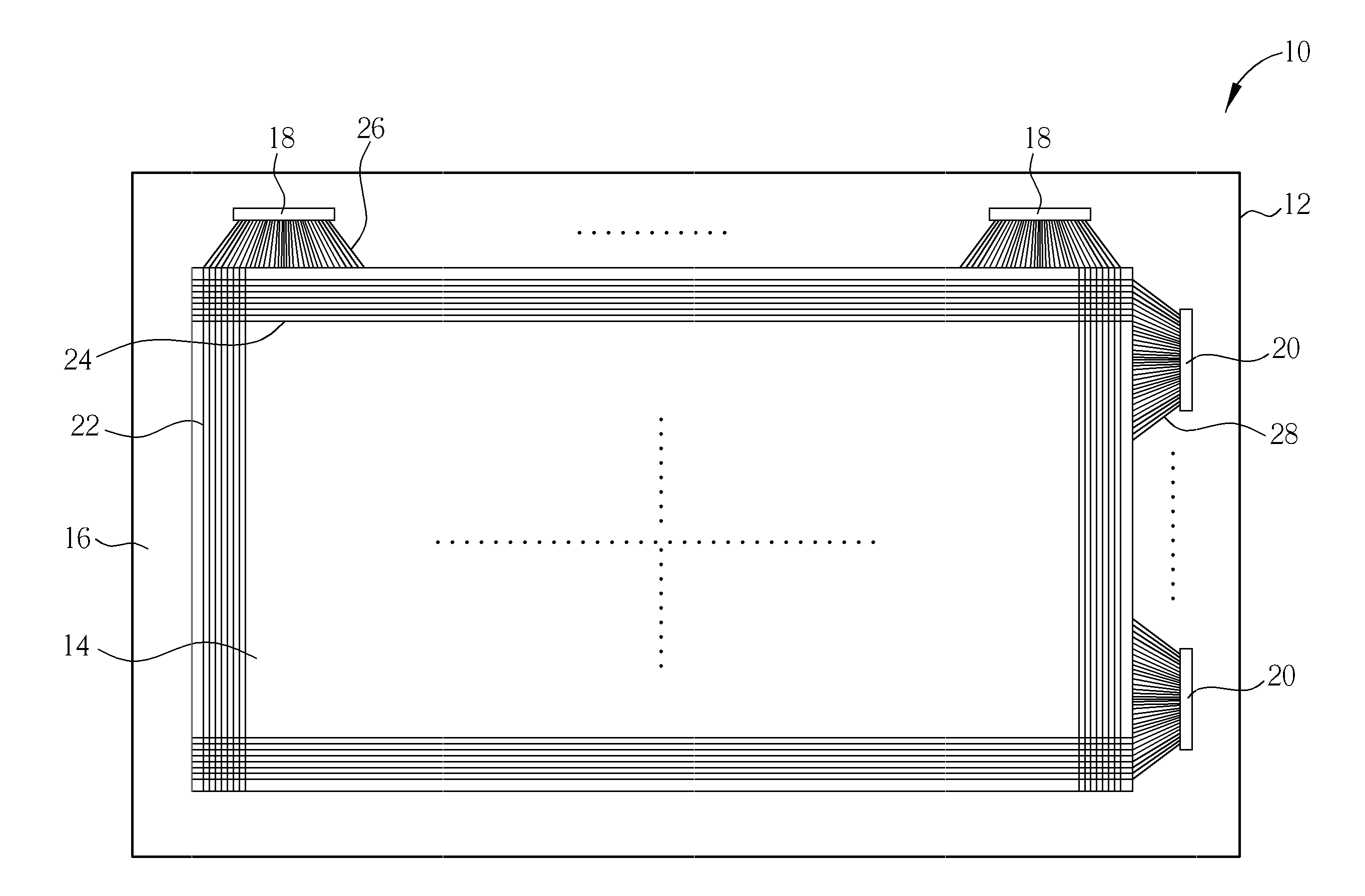
[0018]With reference to FIG. 1 and FIG. 2, FIG. 1 and FIG. 2 are schematic diagrams illustrating a flat display panel of the present invention, wherein FIG. 1 is a schematic diagram illustrating a top view of the flat display panel, and FIG. 2 is an enlarged schematic diagram illustrating parts of devices of FIG. 1. As illustrated in FIG. 1, the flat display panel 10 of the present invention includes a substrate 12. A display area 14 and a peripheral circuit area 16 are defined on the substrate 12, wherein the peripheral circuit area 16 is disposed on at least a side of the display area 14. In this embodiment, the peripheral circuit area 16 surrounds the display area 14. The flat display panel 10 further includes a plurality of driving chips 18, 20 disposed in the peripheral circuit area 16, a plurality of control lines 22, 24 disposed in the display area 14, and a plurality of conductive lines 26, 28 disposed in the peripheral circuit area 16. The conductive lines 26 and the conduc...

third embodiment

[0024]With reference to FIG. 4, FIG. 4 is a schematic diagram illustrating the driving chip and the wiring design of the flat display panel of the present invention, parts of the components are denoted by identical numerals shown in FIG. 2 and FIG. 3. In this embodiment, parts of the conductive lines 26 have winding regions 32 with wavelike shape pattern disposed in the peripheral circuit area. In the winding regions 32, the wave amplitudes e.g. A1, A2 of the conductive lines 26 stand for the lengths of one wavelike shape. Wherein, the wave amplitude is defined as the distance between a midpoint of a wave crest and a wave trough and another adjacent midpoint of a wave crest and a wave trough. In order to clearly explain the definition of wave amplitudes A1, A2, FIG. 5 is provided to show an enlarged schematic diagram illustrating parts of the conductive lines 26n. As illustrated in FIG. 5, the wave crest E1 and the wave trough T1 adjacent to each other have a midpoint M1, and the mi...

fourth embodiment

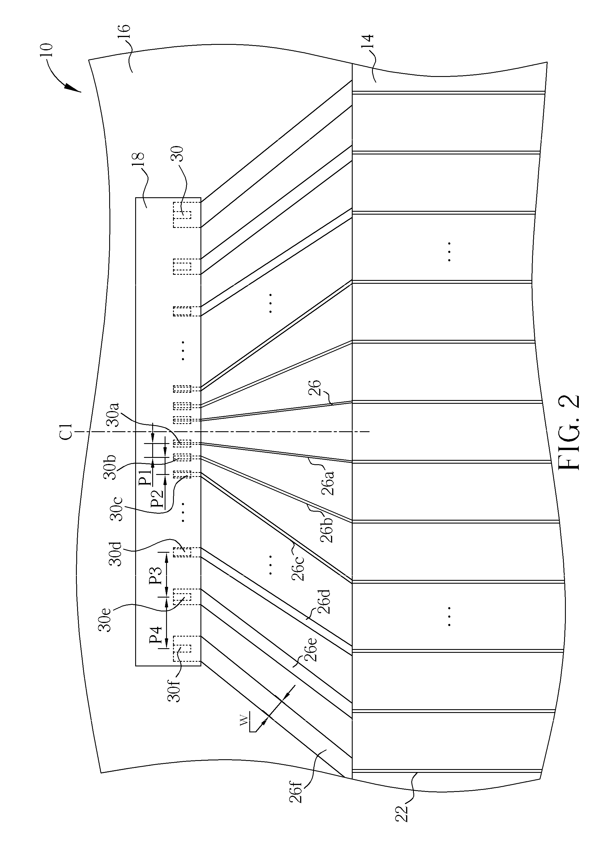
[0025]With reference to FIG. 6, FIG. 6 is a schematic diagram illustrating the driving chip and the wiring design of the flat display panel of the present invention. Similar to the aforementioned embodiment, the pitches of the pins 30 of the driving chip 18 are incompletely identical. For instance, the pitches of the pins 30 in the border portion of the driving chip 18 are larger, and the pitches of the pins 30 in the central portion of the driving chip 18 are smaller. In this embodiment, each of the conductive lines 26 is corresponding to a pin 30 and has an identical width. In addition, each of the conductive lines 26 has a winding region 32 including wiring design with a serrated shape pattern. As a result, the wave amplitudes e.g. A1 of the conductive lines 30 near the central line C1 are smaller, and the conductive lines 26 corresponding to the pins 30 in the border portion or near the edge of the driving chip 18 have larger wave amplitudes.


PUM


Abstract

A flat display panel includes a substrate, at least a driving chip, a plurality of control lines and conductive lines. The substrate has a display area and peripheral circuit area defined thereon. The driving chip is disposed in the peripheral circuit area, and has a plurality of pins. The pitches of adjacent pins are varied. The pitches of the pins in the central portion of the driving chip are smaller than the pitches of the pins in the border portion. The control lines and the conductive lines are disposed in the display area and the peripheral circuit area respectively, and the control lines are electrically connected to the conductive lines.

Description

BACKGROUND OF THE INVENTION[0001]1. Field of the Invention[0002]The present invention relates to a flat display panel, and more particularly, to a flat display panel having a driving chip including pins with nonequivalent pitches.[0003]2. Description of the Prior Art[0004]In comparison with traditionally non-planar displays such as cathode ray tube (CRT) display, flat displays possess advantages of low weight and thin thickness. In view of this, the flat display has gradually become a trendy product, for instance, in domestic televisions, personal computer displays, and portable electronic products e.g. mobile phones, digital cameras and portable music player devices. According to different display techniques, various types of flat displays may be, plasma display panels (PDPs), liquid crystal displays (LCDs) and organic light emitting diode (OLED) displays. In general, the aforementioned flat displays have electronic devices or illumination devices installed on the thin type substra...

Claims


Application Information

Patent Timeline
IPC IPC(8): G09G5/00
CPCG09G2300/0426G09G3/20
Inventor FU, CHIEN-HAOCHIANG, MIN-FENGLEE, MING-CHINCHANG, CHUN-HUANHSU, PAI-HUNG
Owner AU OPTRONICS CORP
Why Eureka
Try Eureka