Active-matrix substrate, display device, and television receiver
a technology of active matrix and substrate, which is applied in the direction of color television details, television systems, instruments, etc., can solve the problems of undesirable short circuit of storage capacitor wire, and achieve the effect of eliminating the difference in capacitan
- Summary
- Abstract
- Description
- Claims
- Application Information
AI Technical Summary
Benefits of technology
Problems solved by technology
Method used
Image

Examples
embodiment 1
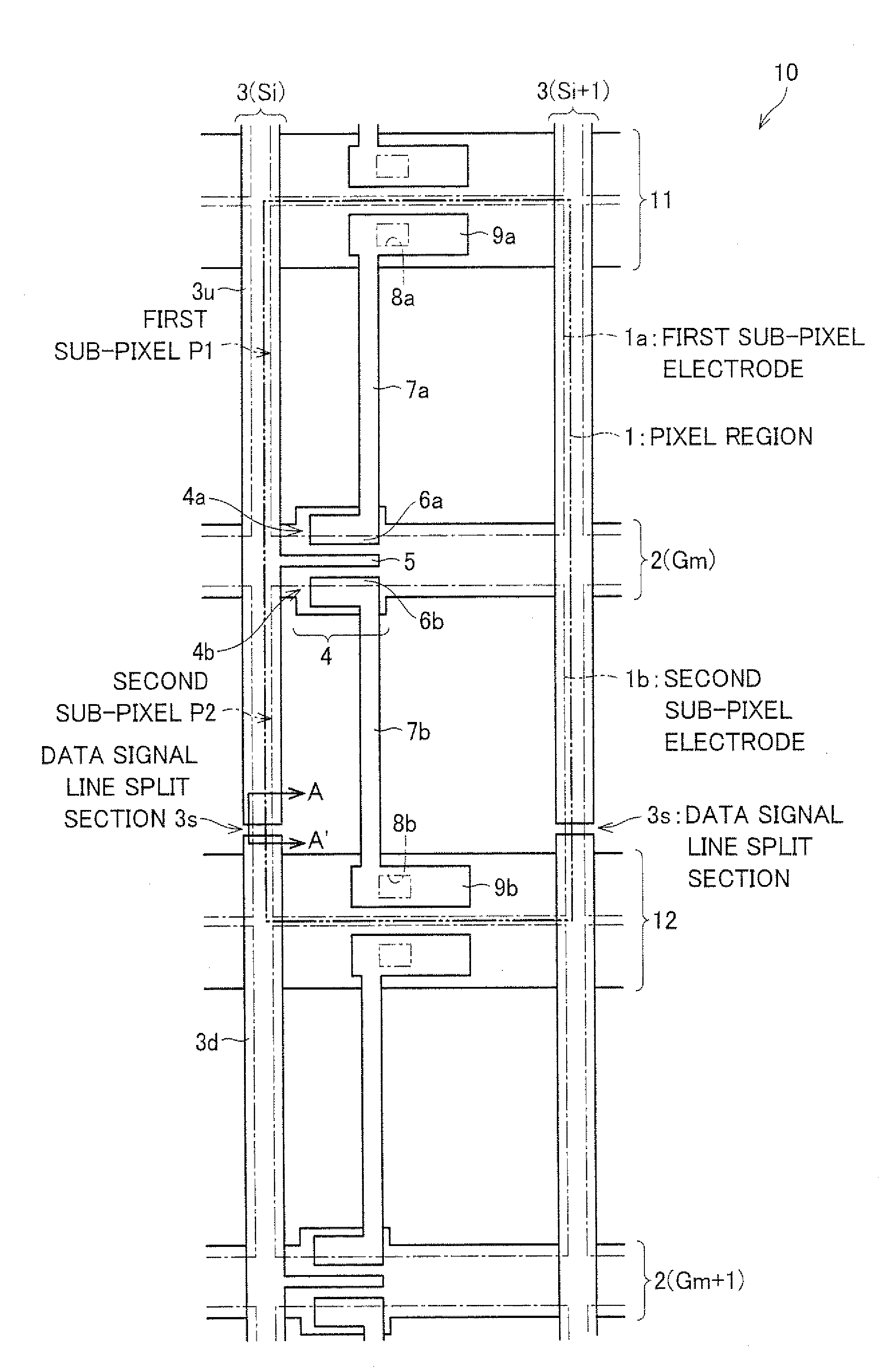
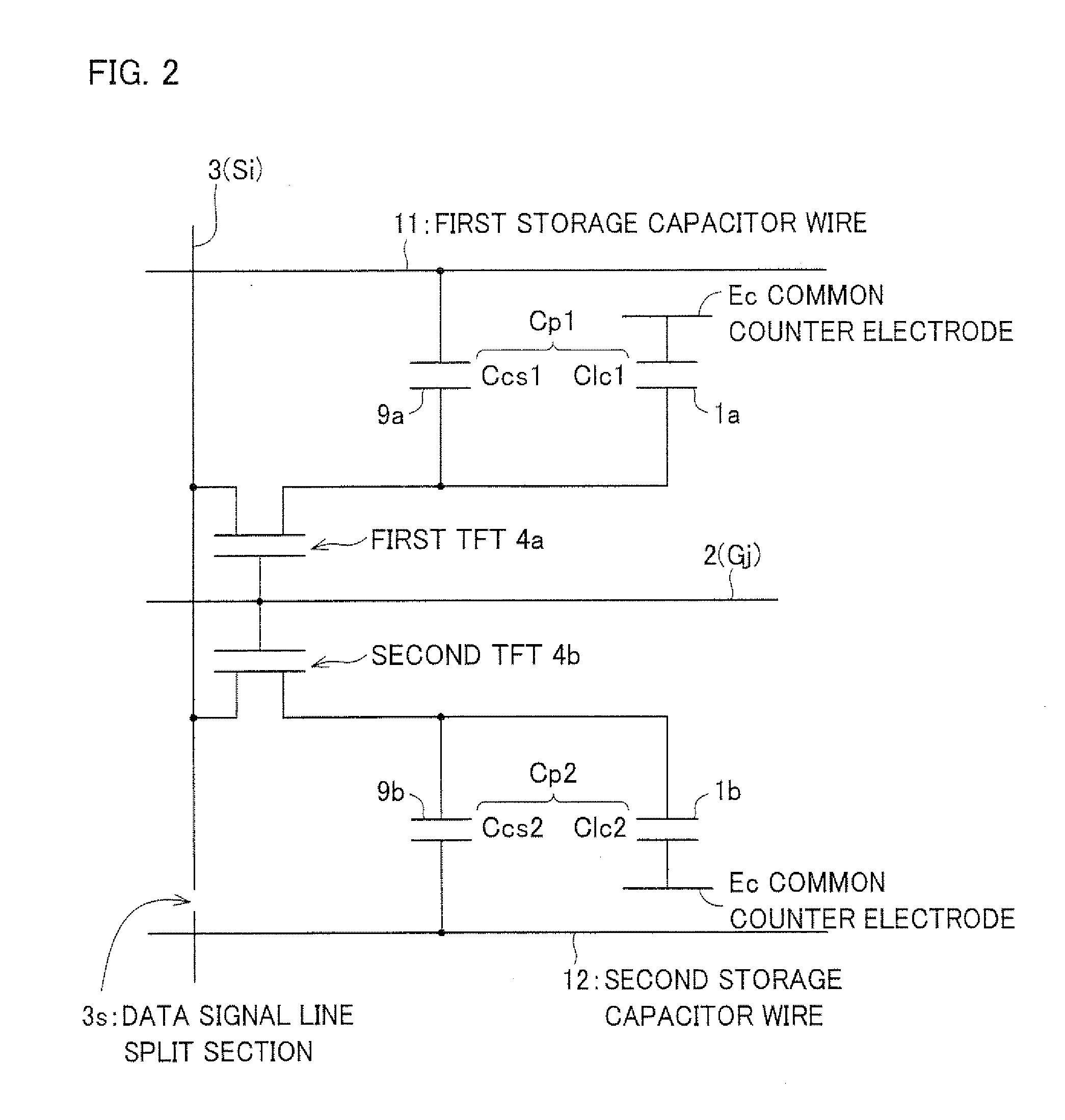
[0109]An embodiment of the present invention will be described below with reference to FIGS. 1 through 10.
[0110]According to the present embodiment, an active-matrix substrate, a liquid crystal display device serving as a display device, and a television receiver each have a so-called multi-pixel structure in which each pixel is split into two or more sub-pixels.
[0111]That is, in the multi-pixel structure, a pixel is split into two or more sub-pixels, and the sub-pixels are driven individually. Such a mode in which a pixel is constituted by two or more sub-pixels is an advantageous mode because a reduction in proportion of normal pixels can be suppressed, for example, even if a correction is made in response to the occurrence of a defect in a pixel.
[0112]Further, in cases where the multi-pixel structure is applied, it is preferable that at least two of the sub-pixels have different luminances. According to this mode, a single pixel contains both a bright sub-pixel and a dark sub-pix...
embodiment 2
[0265]Another embodiment of the present invention will be described below with reference to FIG. 11. It should be noted that arrangements except those described in the present embodiment are the same as those described above in Embodiment 1. Further, for convenience of explanation, members having the same functions as those shown in the figures of Embodiment 1 are given the same reference numerals, and will not be described below.
[0266]FIG. 11 is a plan view of an arrangement of an active-matrix substrate 30 of the present embodiment, and shows the vicinity of a region where each data signal line 3 is split into two parts. The second storage capacitor wire 32 has a second storage capacitor wire notched section 32a, provided near an intersection between the second storage capacitor wire 32 and a data signal line 3, which serves as a notch region. The data signal line 3 is split into two parts at the second storage capacitor wire notched section 32a.
[0267]Therefore, the total capacit...
embodiment 3
[0269]Another embodiment of the present invention will be described below with reference to FIG. 12. It should be noted that arrangements except those described in the present embodiment are the same as those described above in Embodiment 1. Further, for convenience of explanation, members having the same functions as those shown in the figures of Embodiment 1 are given the same reference numerals, and will not be described below.
[0270]FIG. 12 is a plan view of an arrangement of an active-matrix substrate 40 of the present embodiment, and shows the vicinity of a region where each data signal line 3 is split into two parts.
[0271]The present embodiment has the same position of a data signal line split section 3s as Embodiment 1. However, in the active-matrix substrate 40 of the present embodiment, the second sub-pixel electrode 1b has a pixel electrode notched section 41, provided in the position of the data signal line split section 3s, which serves as a notch region.
[0272]Therefore,...
PUM
 Abstract
Description
Claims
Application Information