Warp-suppressed semiconductor device

a semiconductor and resistance-suppression technology, applied in semiconductor devices, semiconductor/solid-state device details, electrical devices, etc., can solve the problem of limiting the stress caused by the contraction/expansion of the first resin to a minimum, and achieve the effect of suppressing the deformation of the mounting substra

Inactive Publication Date: 2010-09-16
RENESAS ELECTRONICS CORP
View PDF39 Cites 53 Cited by
  • Summary
  • Abstract
  • Description
  • Claims
  • Application Information

AI Technical Summary

Benefits of technology

[0019]An object of the present invention is to provide a semiconductor device including a semiconductor chip mounted on a mounting substrate through flip chip bonding, in which, in a state after sealing, the amount of warpage in the mounting substrate is in a range which does not hinder solder-mounting of the semiconductor device on a mounting board such as a circuit board; in a temperature cycling test, no destruction is caused by the occurrence of cracks, detachment and the like in solder bumps and the like which are connecting members between the semiconductor chip and the mounting substrate; and no cracks and the like occur in the mounting substrate.
[0021]According to the semiconductor device thus configured, by selecting the first resin and the second resin so that a thermal expansion coefficient of the second resin is smaller than that of the first resin, it is possible to relax the contraction / expansion stress of the first resin caused by temperature changes during and after heat curing. Accordingly, warpage in the mounting substrate can be suppressed even if a material with low viscosity but with a slightly high thermal expansion coefficient is used for the first resin in order to prevent the occurrence of voids in the underfill part and to suppress detachment and destruction of the connection members. Moreover, even in a temperature cycling test in which a low temperature state and a high temperature state are repeated by turns, stress caused by the contraction / expansion of the first resin is limited to a minimum. Thus, it is possible to prevent the occurrence of cracks, detachment and destruction in the connection members such as solder bumps, and detachment of the chip electrodes and the internal land electrodes. More preferably, the thermal expansion coefficient of the second resin is smaller than that of the mounting substrate.
[0023]According to this manufacturing method, since the strength of the mounting substrate can be reinforced, it is possible to improve handling performance during the manufacturing processes and to suppress warpage in the mounting substrate. Moreover, since the adhesives and the resins are temporarily cured in the respective steps to become in a semi-cured state, and subjected to real curing at the end to be completely cured, it is possible to suppress warpage in the mounting substrate after the manufacture to a minimum.
[0025]According to this manufacturing method, since the second resin is injected and cured after the lid is attached, the space can be completely filled with the second resin without generating any empty space in the vicinity of the lid, and thus deformation of the mounting substrate can be suppressed.

Problems solved by technology

Moreover, even in a temperature cycling test in which a low temperature state and a high temperature state are repeated by turns, stress caused by the contraction / expansion of the first resin is limited to a minimum.

Method used


Image

  • Warp-suppressed semiconductor device
  • Warp-suppressed semiconductor device
  • Warp-suppressed semiconductor device

Examples


first embodiment

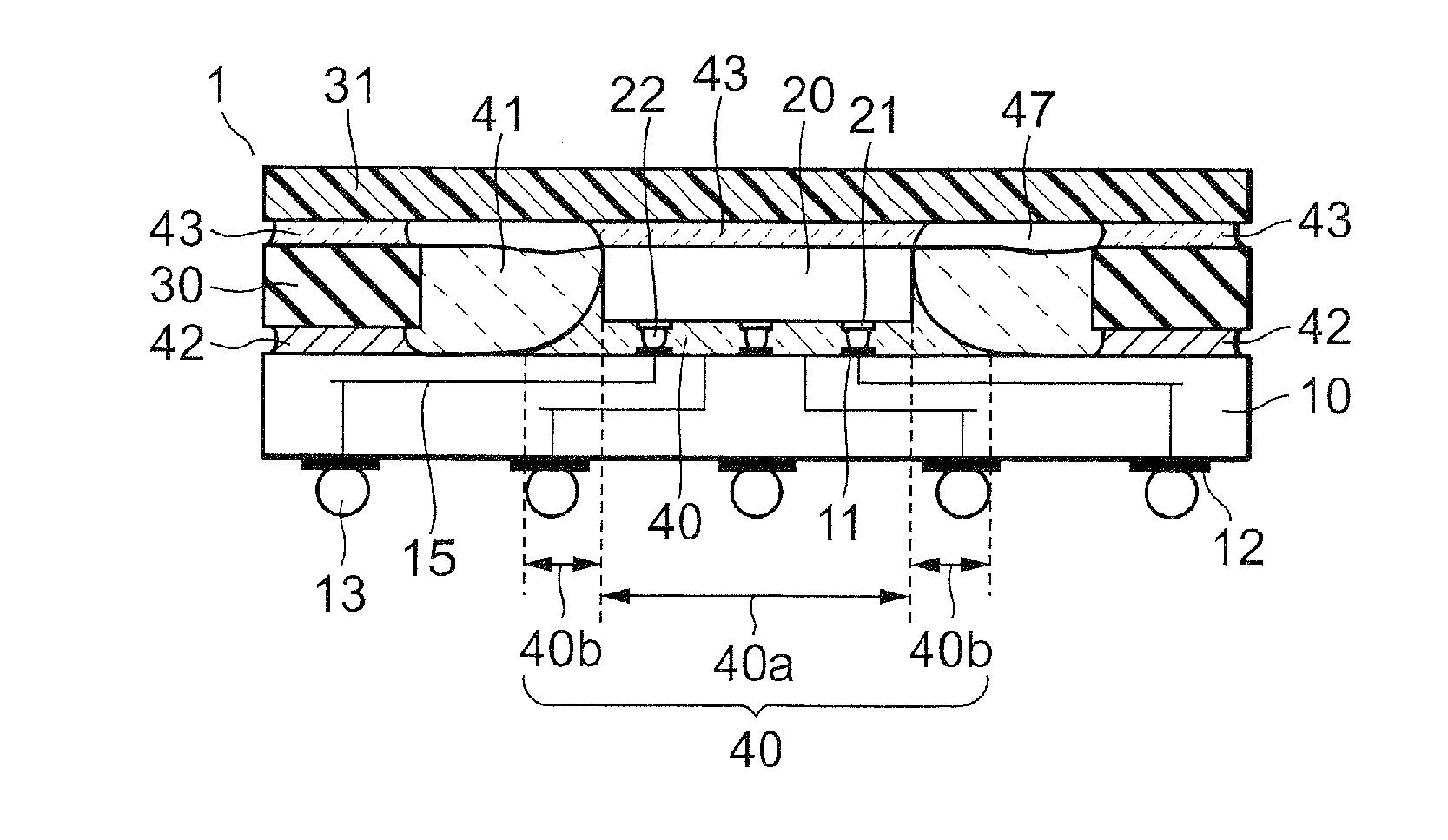
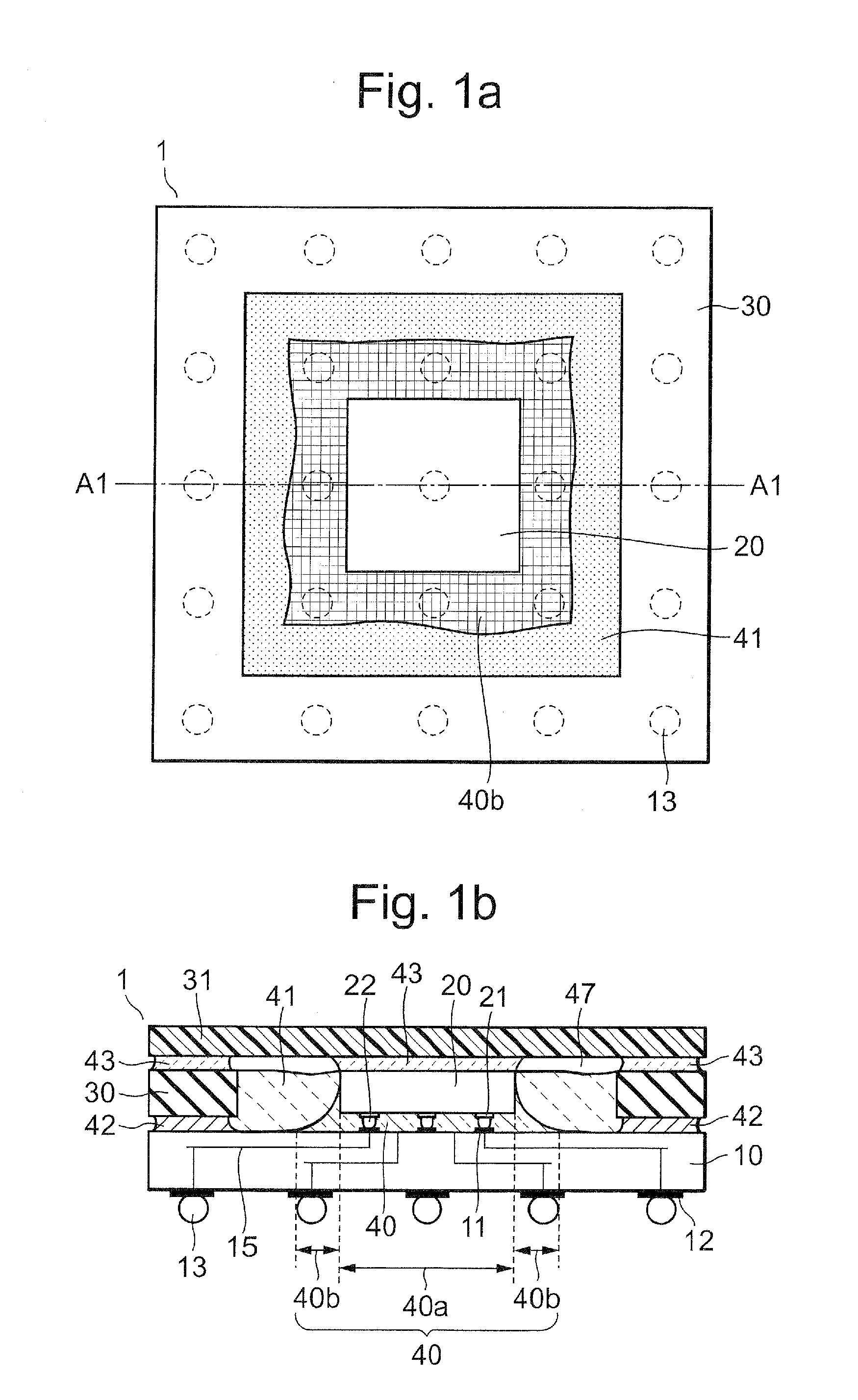
[0052]As shown in FIGS. 1a and 1b, a semiconductor device 1 of a first embodiment includes: a mounting substrate 10; a semiconductor chip 20, mounted on a first surface of the substrate 10 through flip chip bonding; a first resin 40 filling a gap between the substrate 10 and the chip 20; a frame-shaped stiffener 30 surrounding the chip 20; a first adhesive 42 for bonding a first end surface of the stiffener 30 to the substrate 10; a lid 31 for covering the stiffener 30 and an area surrounded by the stiffener 30; a second adhesive 43 for bonding the lid 31 to a backside of the chip 20 and to a second end surface opposite the first end surface of the stiffener 30; and a second resin 41 filling a space between the stiffener 30 and the chip 20 in contact with the first resin 40. The first resin 40 includes an underfill part 40a filling a gap between the chip 20 and the substrate 10, and a fillet part 40b extended from a region where the chip 20 and the substrate 10 face each other. Deta...

second embodiment

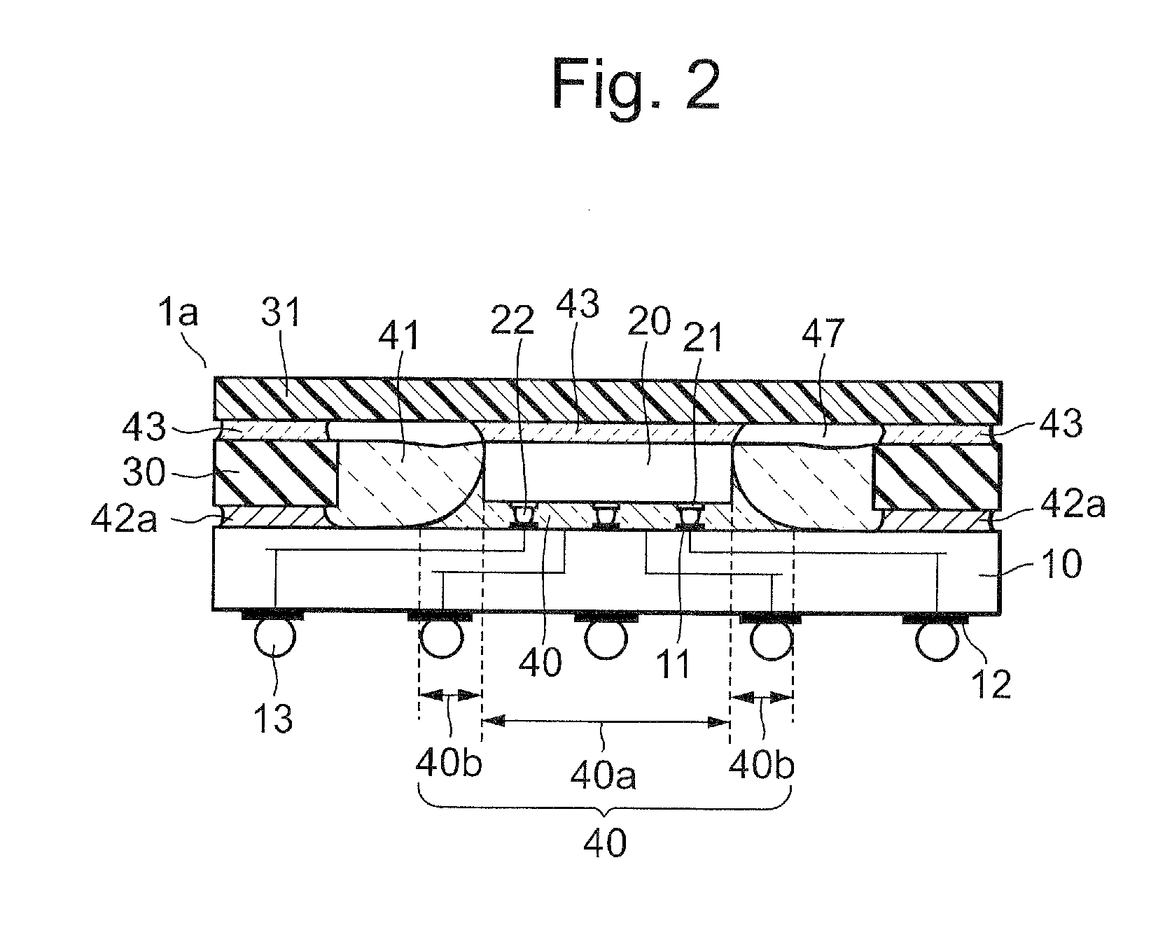
[0066]Next, a second embodiment will be described with reference to FIG. 2. Note that a method for manufacturing a semiconductor device 1a of the second embodiment is similar to that for the semiconductor device 1 of the first embodiment. A configuration of the semiconductor device 1a is almost the same as that of the semiconductor device 1. The difference between the semiconductor device 1a and the semiconductor device 1 is that a resin the same as the second resin 41 is used as a first adhesive 42a for bonding the stiffener 30 to the substrate 10. According to this semiconductor device 1a, by using the resin the same as the second resin 41 with a thermal expansion coefficient of about 8 to 16 ppm and with an elastic modulus of 11 to 28 GPa for the first adhesive 42a for bonding the stiffener 30, the contraction in a portion of the substrate 10 directly facing the chip 20 can be reduced more, and thus it is possible to suppress the warpage in the substrate 10.

third embodiment

[0067]Next, a third embodiment will be described with reference to FIGS. 3a to 3c. Referring to FIGS. 3a to 3c, a semiconductor device 1b of the third embodiment includes: a mounting substrate 10; a semiconductor chip 20 mounted on a first surface of the substrate 10 through flip chip bonding; a first resin 40 filling a gap between the substrate 10 and the chip 20; a frame-shaped stiffener 32 surrounding the chip 20; a first adhesive 42 for bonding a first end surface of the stiffener 32 to the substrate 10; a lid 31 for covering the stiffener 32 and an area surrounded by the stiffener 32; a second adhesive 43 for bonding the lid 31 to a backside of the chip 20 and to a second end surface opposite the first end surface of the stiffener 32; and a second resin 41 filling a space surrounded by the stiffener 32, side faces of the chip 20 and the substrate 10 in contact with the first resin 40. The first resin 40 includes an underfill part 40a filling a gap between the chip 20 and the su...


PUM


Abstract

A semiconductor device includes: a semiconductor chip mounted on a mounting substrate; a first resin filling a gap between the chip and the substrate; a frame-shaped stiffener surrounding the chip; a first adhesive for bonding the stiffener to the substrate; a lid for covering the stiffener and an area surrounded by the stiffener; and a second resin filling a space between the stiffener and the chip. A thermal expansion coefficient of the second resin is smaller than that of the first resin. The first resin includes an underfill part filling a gap between the chip and the substrate and a fillet part extended from the chip region.

Description

BACKGROUND OF THE INVENTION[0001]1. Field of the Invention[0002]This invention relates to a semiconductor device of, e.g., a ball grid array (BGA) type, in which a semiconductor chip is connected, through flip chip bonding, to a mounting substrate manufactured by the same method as that for an organic printed wiring board, and a method for manufacturing the same.[0003]2. Description of the Related Art[0004]Generally, a mounting substrate to which the semiconductor chip is connected through flip chip bonding is manufactured by the same method as that for an organic printed wiring board. The mounting substrate is formed of wiring layers the number of which ranges from two to a dozen or so depending on purposes. However, the thickness of the mounting substrate is about 0.5 to 2.0 m even if there are a dozen wiring layers or so. Accordingly, the mounting substrate is very vulnerable to external force or stress caused by a difference in coefficients of thermal expansion between materials...

Claims


Application Information

Patent Timeline
Patent Type & Authority Applications(United States)
IPC IPC(8): H01L23/16H01L23/12H01L21/56H01L23/10H01L23/24H01L23/28
CPCH01L21/563H01L23/10H01L2224/32225H01L2924/01033H01L2924/01006H01L2924/3511H01L2924/18161H01L2924/16195H01L2924/15311H01L2924/15174H01L2924/12044H01L2924/01082H01L2924/01079H01L2924/01057H01L2924/01047H01L2924/01039H01L2924/01029H01L23/24H01L24/28H01L2224/16225H01L2224/73203H01L2224/73204H01L2224/73253H01L2224/83102H01L2224/92125H01L2924/01002H01L2924/01004H01L2924/01005H01L2924/01013H01L2924/3512H01L2924/00H01L2924/00012H01L2224/05573H01L2224/05568H01L2924/00014H01L23/16H01L23/562H01L2224/05599H01L23/28
Inventor HONDA, HIROKAZU
Owner RENESAS ELECTRONICS CORP
Why Eureka
Try Eureka