Electronic component and passive component

a passive component and electronic component technology, applied in the field of electronic components, can solve the problems of insufficient disclosure of patent documents 1 through 4 described above, interference problems, and the size of the inductor becomes larger, and achieve the effect of low power consumption and low loss

Active Publication Date: 2010-09-16
SOSHIN ELECTRIC
View PDF4 Cites 1 Cited by
  • Summary
  • Abstract
  • Description
  • Claims
  • Application Information

AI Technical Summary

Benefits of technology

[0015]The present invention has been made in view of the aforementioned difficulties. It is an object of the present invention to provide an electronic component and a passive component, which enable an inductor to be small in size, and at the same time to further increase the Q factor of the inductor, thereby achieving attenuation in adjacent frequency bands, and realizing a low power consumption level based on low loss, by clarifying the correlation of the distance between a pair of identical patterns and the distance between pairs of identical patterns that are adjacent to each other along a direction in which they are stacked.
[0022]As described above, the electronic component and the passive component according to the present invention are capable of further increasing the Q factor of an inductor, thereby achieving attenuation in adjacent frequency bands, and realizing a low power consumption level based on low loss, by clarifying a correlation between the distance between a pair of identical patterns, and the distance between pairs of identical patterns that are adjacent to each other along a direction in which they are stacked.

Problems solved by technology

Controlling a reduction in the inductance value requires an increase in the number of turns of the inductor patterns and / or an increase in the turn diameter, thus causing a problem in that the inductor becomes larger in size.
Communication terminal devices in recent years have adjacent frequency bands used by applications (GPS, television, wireless communications, etc.) run thereby, resulting in an interference problem.
The disclosures of Patent Documents 1 through 4 described above are not sufficient to meet these requirements, and further study is needed.

Method used


Image

  • Electronic component and passive component
  • Electronic component and passive component
  • Electronic component and passive component

Examples


Embodiment Construction

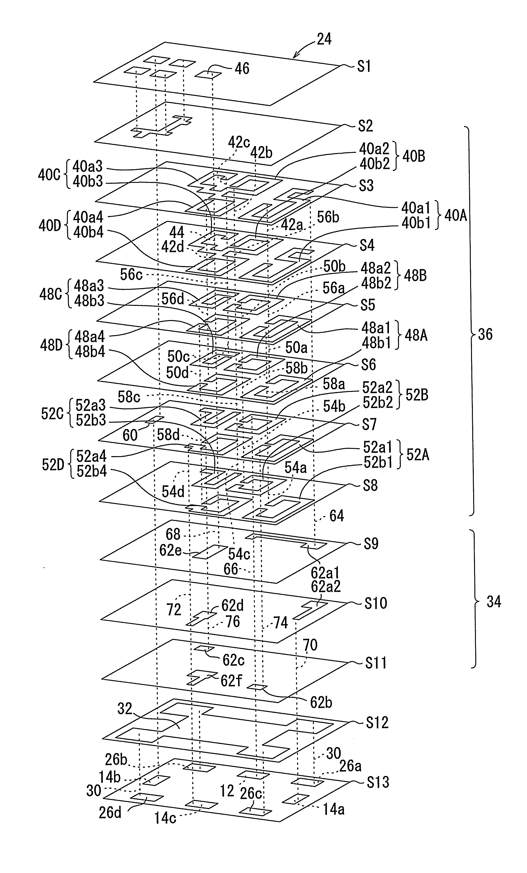
[0041]Embodiments of an electronic component according to the present invention, which is applied to a passive component, will be described below with reference to FIGS. 1 through 18.

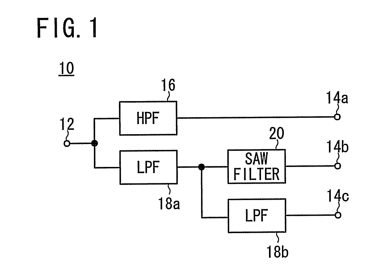
[0042]As shown in FIG. 1, a passive component 10 according to an embodiment of the present invention comprises a triplexer, having a single input terminal 12 and three output terminals (first through third output terminals 14a through 14c).

[0043]A high-pass filter 16 is connected between the input terminal 12 and the first output terminal 14a. A first low-pass filter 18a and a SAW filter 20 are connected in series between the input terminal 12 and the second output terminal 14b. The first low-pass filter 18a and a second low-pass filter 18b are connected in series between the input terminal 12 and the third output terminal 14c.

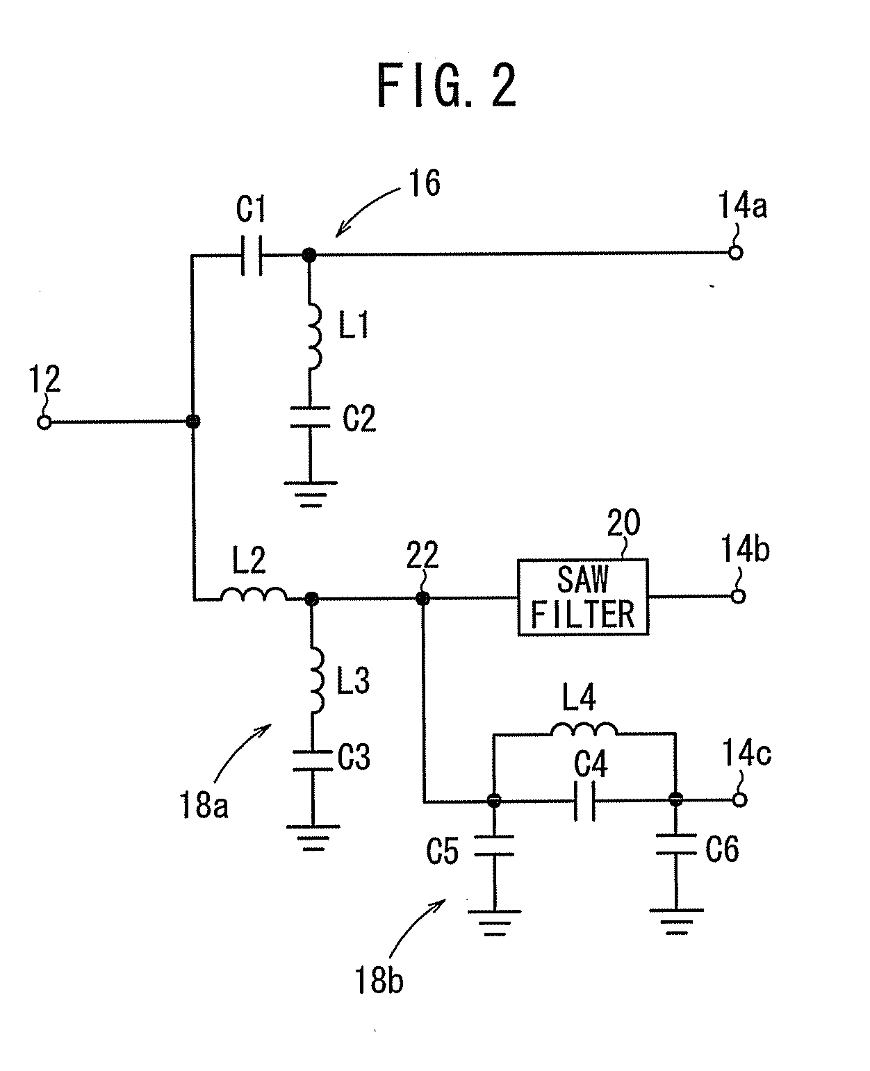
[0044]FIG. 2 shows a structural example of the circuit of the passive component 10. The high-pass filter 16 comprises a first capacitor C1 connected between the input terminal 12...


PUM

PropertyMeasurementUnit
Daaaaaaaaaaa
distanceaaaaaaaaaa
conductiveaaaaaaaaaa

Abstract

An electronic component and a passive component define correlation between a distance between a pair of identical patterns and a distance between pairs of identical patterns adjacent to each other in a laminating direction, and a value of an inductor is further improved, attenuation in adjacent frequency bands is ensured and low power consumption is achieved with low loss. A first inductor is composed of a pair of inductor forming electrodes, a pair of inductor forming electrodes and a pair of inductor forming electrodes. A relationship between a distance (Da) between the two electrodes configuring each pair of inductor forming electrodes and a distance (Db) between the pairs of inductor forming electrodes adjacent to each other in the laminating direction satisfy the following inequalities; 0<Da≦Db and 0<Da≦20 μm.

Description

TECHNICAL FIELD[0001]The present invention relates to an electronic component having inductors disposed in a dielectric substrate, which is made up of a plurality of laminated dielectric layers, and to a passive component utilizing such an electronic component. More particularly, the present invention concerns an electronic component and a passive component, which are suitable for use in a filter such as a low-pass filter, a bandpass filter, a high-pass filter, or the like, and a triplexer incorporating such a filter or the like.BACKGROUND ART[0002]Heretofore, electronic components have been known having inductors disposed in a dielectric substrate, which is made up of a plurality of laminated dielectric layers. Patent Documents 1 through 4, for example, have been proposed particularly for improving the Q factor of such inductors.[0003]The electronic component disclosed in Patent Document 1 has three conductive patterns having substantially identical shapes disposed in a dielectric ...

Claims


Application Information

Patent Timeline
Patent Type & Authority Applications(United States)
IPC IPC(8): H03H7/01H01F17/00
CPCH01F17/0006H03H2001/0085H03H7/463
Inventor TAKASE, KOUHEI
Owner SOSHIN ELECTRIC
Why Eureka
Try Eureka