Unlock instant, AI-driven research and patent intelligence for your innovation.

Image sensor and image capturing apparatus

a technology of image sensor and image capturing apparatus, which is applied in the direction of television system, radiation control device, color signal processing circuit, etc., can solve the problems of image quality deterioration, poor image quality, and noise generated in ob pixel also generating horizontal streak noise, so as to reduce the noise contained

Inactive Publication Date: 2010-09-16
CANON KK
View PDF11 Cites 19 Cited by
  • Summary
  • Abstract
  • Description
  • Claims
  • Application Information

AI Technical Summary

Benefits of technology

[0020]The present invention has been made to overcome the conventional drawbacks, and implements a technique to reduce noise contained in a reference signal for black level read out from a reference pixel for black level.

Problems solved by technology

The clamp circuit malfunctions, causing the image quality to deteriorate.
The presence of even a small defect results in poor image quality.
Noise generated in an OB pixel also generates horizontal streak noise.
However, this method decreases the yield of the image sensor and raises the cost because the defect determination level in the OB region is set stricter than that in the normal effective pixel region.
However, variations in the threshold of the transistor of a circuit arranged on each vertical signal line generate noise that differs between columns.
More specifically, as the amplification transistor is miniaturized to decrease the gate width or gate length, noise generated in the amplification transistor increases.
Even in an image sensor using a CMOS image sensor, a smaller pixel area increases noise generated in the amplification transistors of pixel amplifiers in the effective pixel region and OB region, as described above.
If the amount of noise that is generated in the amplification transistor of a pixel amplifier and contained in a reference pixel for black level increases, the clamp precision decreases, deteriorating the image quality.
Hence, if the amount of noise which is generated in the amplification transistor of a pixel amplifier and contained in a reference pixel for black level increases, the correction precision decreases, deteriorating the image quality.
In Japanese Patent Laid-Open No. 2005-223860, because the amplification transistor of a pixel amplifier operates differently from a pixel, the same signal as that containing vertical streak noise generated in a pixel cannot be obtained, impeding accurate correction.

Method used


Image

  • Image sensor and image capturing apparatus
  • Image sensor and image capturing apparatus
  • Image sensor and image capturing apparatus

Examples


first embodiment

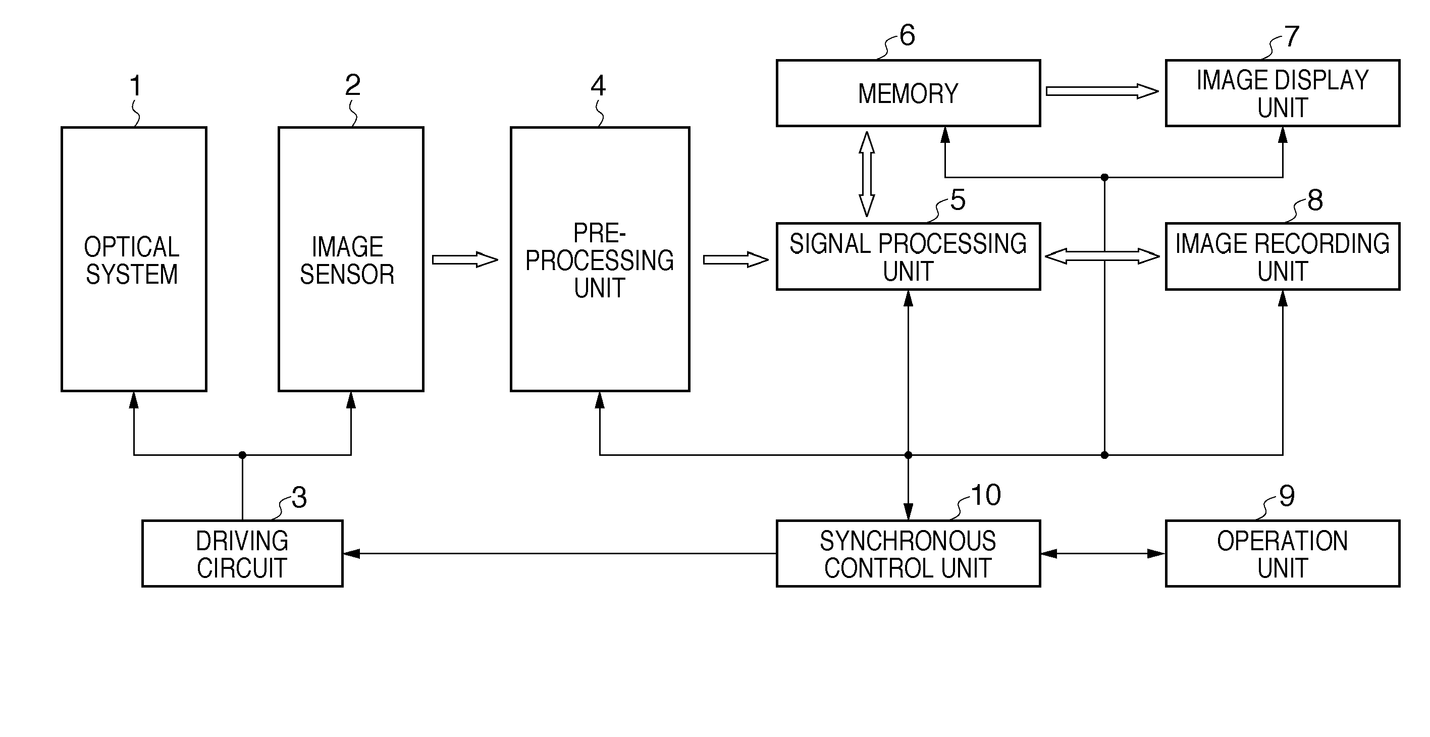
[0110]The first embodiment of the present invention will be explained with reference to FIGS. 5 to 9 in addition to FIGS. 1 to 4.

[0111]FIG. 5 is a view showing the pixel array of an image sensor 2 in the first embodiment of the present invention.

[0112]In an effective pixel region 60, photosensitive pixels (FIG. 3) having photo-electric conversion elements are arrayed. In a first OB region 61, light-shielded pixels (first reference pixels for black level) are arrayed. In a second OB region 62, light-shielded pixels (second reference pixels for black level) are arrayed. In FIG. 2, the pixel count of the image sensor 2 is three in both the horizontal and vertical directions for descriptive convenience of the operation. In FIG. 5, the image sensor 2 is assumed to include pixels many enough to perform an OB clamp operation and vertical streak noise correction operation.

[0113]FIG. 6 is a view of the layout of a photosensitive pixel (FIG. 3) having a photo-electric conversion element. FIG....

second embodiment

[0145]An image capturing apparatus according to the second embodiment of the present invention will be explained with reference to FIG. 10 in addition to FIGS. 1 to 9. In the second embodiment, the basic arrangement and operation of the image capturing apparatus and those of an image sensor are the same as those in the first embodiment. The second embodiment will be explained by applying the same drawings and reference numerals as those in the first embodiment.

[0146]FIG. 10 is a view of the layout of the second light-shielded pixel having a photo-electric conversion element. The same reference numerals and symbols as those in FIG. 8 denote the same parts. Although the pixel is shielded from light, a light-shielding means 801 is not illustrated. The light-shielded pixel has the same section as that in FIG. 7.

[0147]A second light-shielded pixel 920 has a photo-electric conversion element. The second light-shielded pixel 920 is equal in horizontal and vertical lengths to a photosensiti...

third embodiment

[0162]An image capturing apparatus according to the third embodiment of the present invention will be explained with reference to FIGS. 11 to 13 in addition to FIGS. 1 to 10. In the third embodiment, the basic arrangement and operation of the image capturing apparatus and those of an image sensor are the same as those in the first and second embodiments. The third embodiment will be explained by applying the same drawings and reference numerals as those in the first and second embodiments.

[0163]FIG. 11 is a view showing a light-shielded pixel having no photo-electric conversion element. A portion surrounded by a dotted line is a light-shielded pixel 93. The light-shielded pixel 93 has the same structure as that of the pixel in FIG. 3 except that it has a light-shielding means 801 and does not include a photo-electric conversion element D1.

[0164]FIG. 12 is a view of the layout of the third light-shielded pixel having no photo-electric conversion element. This layout is obtained by re...


PUM


Abstract

An image sensor having a pixel amplifier reduces noise generated by a driving transistor (Td1) by setting the gate width (channel width: W) and gate length (channel length: L) of the driving transistors (Td1) of light-shielded pixels arrayed in the first and second OB regions to be larger than those of photosensitive pixels arrayed in an effective pixel region. When the area of a photo-electric conversion element (D1) of a light-shielded pixel is reduced or light-shielded pixels having no photo-electric conversion unit are arrayed, the gate width (channel width: W) and gate length (channel length: L) can be further increased, further reducing noise.

Description

BACKGROUND OF THE INVENTION[0001]1. Field of the Invention[0002]The present invention relates to a noise reduction technique for a reference pixel for black level (OB pixel) in an image capturing apparatus.[0003]2. Description of the Related Art[0004]Today, advanced image sensors have significantly developed image capturing apparatuses such as an electronic still camera and video camera. An image sensor typified by a CMOS (Complementary Metal Oxide Semiconductor) includes a pixel array in which pixels are arrayed in the row and column directions. The image sensor is formed from an effective pixel region where photosensitive pixels are arranged and an OB region where reference pixels for black level (OB pixels) are shielded from light. An image capturing apparatus using the image sensor comprises an OB clamp circuit using OB pixels to remove the DC component of a dark current that greatly varies upon a change of conditions such as the temperature, and low-frequency variations upon po...

Claims


Application Information

Patent Timeline
IPC IPC(8): H04N9/64H04N5/335H01L27/146H04N5/341H04N5/357H04N5/369H04N5/374H04N5/378
CPCH01L27/14603H01L27/14623H04N5/367H04N5/23245H04N5/361H01L27/14645H04N23/667H04N25/68H04N25/633H04N25/63
Inventor YANAI, TOSHIKAZU
Owner CANON KK