Light emitting device

a technology of light-emitting devices and light-emitting layers, which is applied in the direction of solid-state devices, electric lighting sources, and light-emitting sources. it can solve the problems of reducing the luminescence efficiency, affecting the luminescence efficiency, and changing the size of quantum dots, so as to prolong the drive life and prevent the aggregation of qd protected by the protecting material. the effect of the luminescent layer

Inactive Publication Date: 2010-09-23
DAI NIPPON PRINTING CO LTD
View PDF6 Cites 26 Cited by
  • Summary
  • Abstract
  • Description
  • Claims
  • Application Information

AI Technical Summary

Benefits of technology

[0014]The present inventors have aimed at the compatibility between the QD protecting material and the binder component in the luminescent layer as a measure for suppressing a deterioration in brightness of the light emitting device.
[0036]According to the present invention, when the compound contained in the luminescent layer and the QD protecting material contain the moiety A and the moiety B, respectively, while the moiety A and the moiety B satisfy the relationships represented by formulae (I) and (II), the molecule polarity matching between the moiety A and the moiety B is good and the compatibility of the compound contained in the luminescent layer with the QD protecting material is improved, whereby the aggregation of QD protected by the protecting material can be prevented and the protected QD can be homogeneously dispersed in the luminescent layer. Thus, light emitting devices can be provided that have a prolonged drive lifetime and a high color purity and can easily be produced.

Problems solved by technology

The quantum dots, however, are an inorganic structure and thus are disadvantageous in that mixing the quantum dots with a solvent containing the organic binder component in the luminescent layer to prepare a solution causes phase separation to form an aggregate of quantum dots which causes a change in size of the quantum dots.
A change in the size of the quantum dots poses problems such as a change in luminescence wavelength or extinction which makes it impossible to provide a desired color and / or a lowering in luminescence efficiency due to a lowering in internal quantum efficiency by the extinction and / or a change in transport properties of carriers which leads to a higher voltage or a change in carrier balance which leads to a lowered luminescence efficiency.

Method used


Image

  • Light emitting device
  • Light emitting device
  • Light emitting device

Examples


example 1

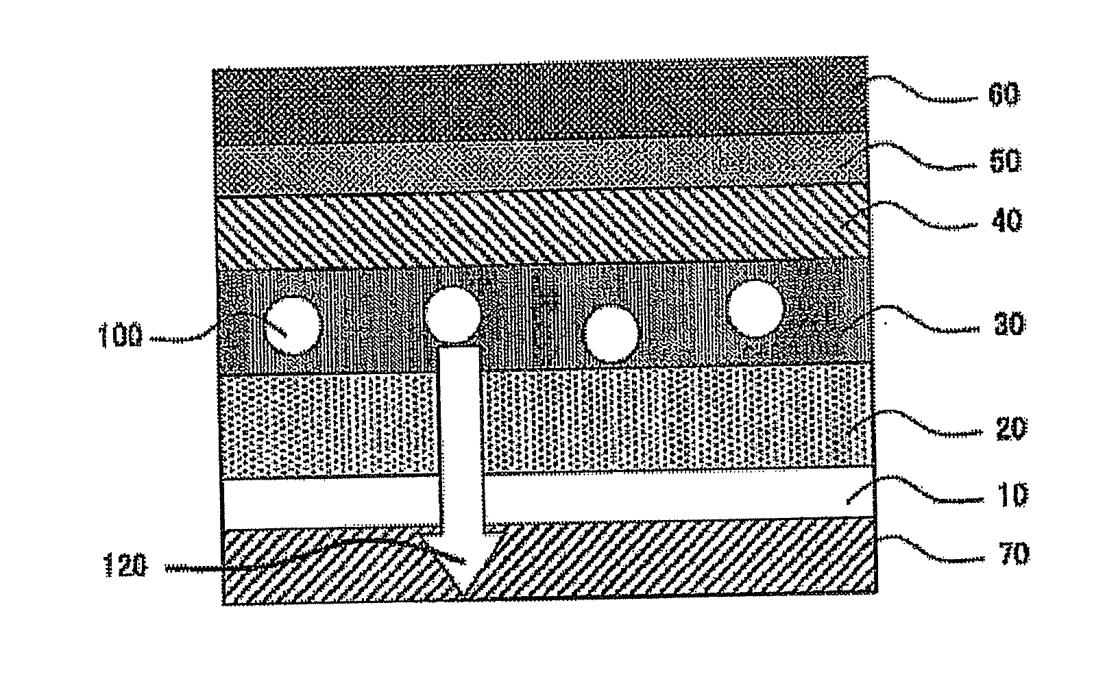
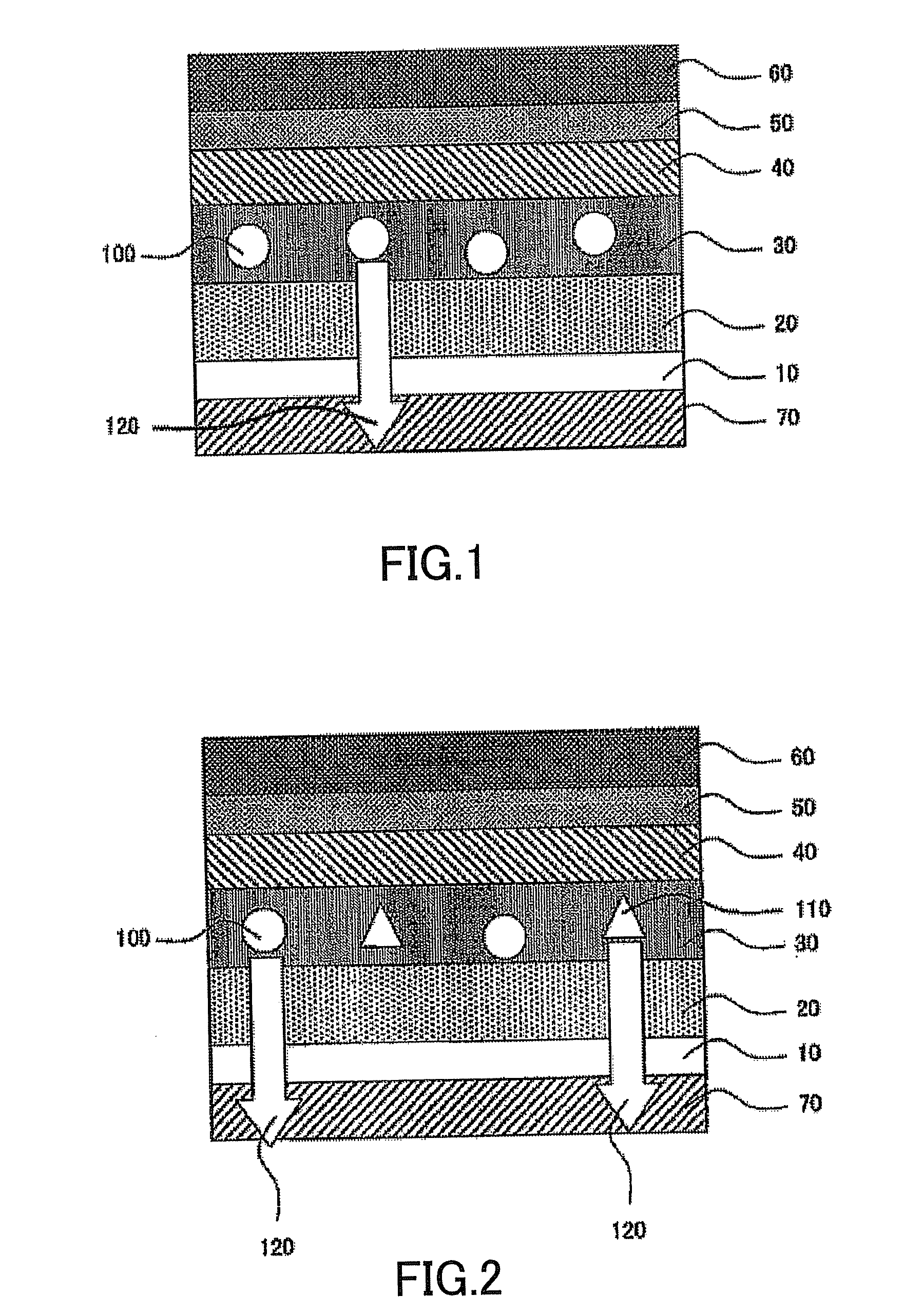
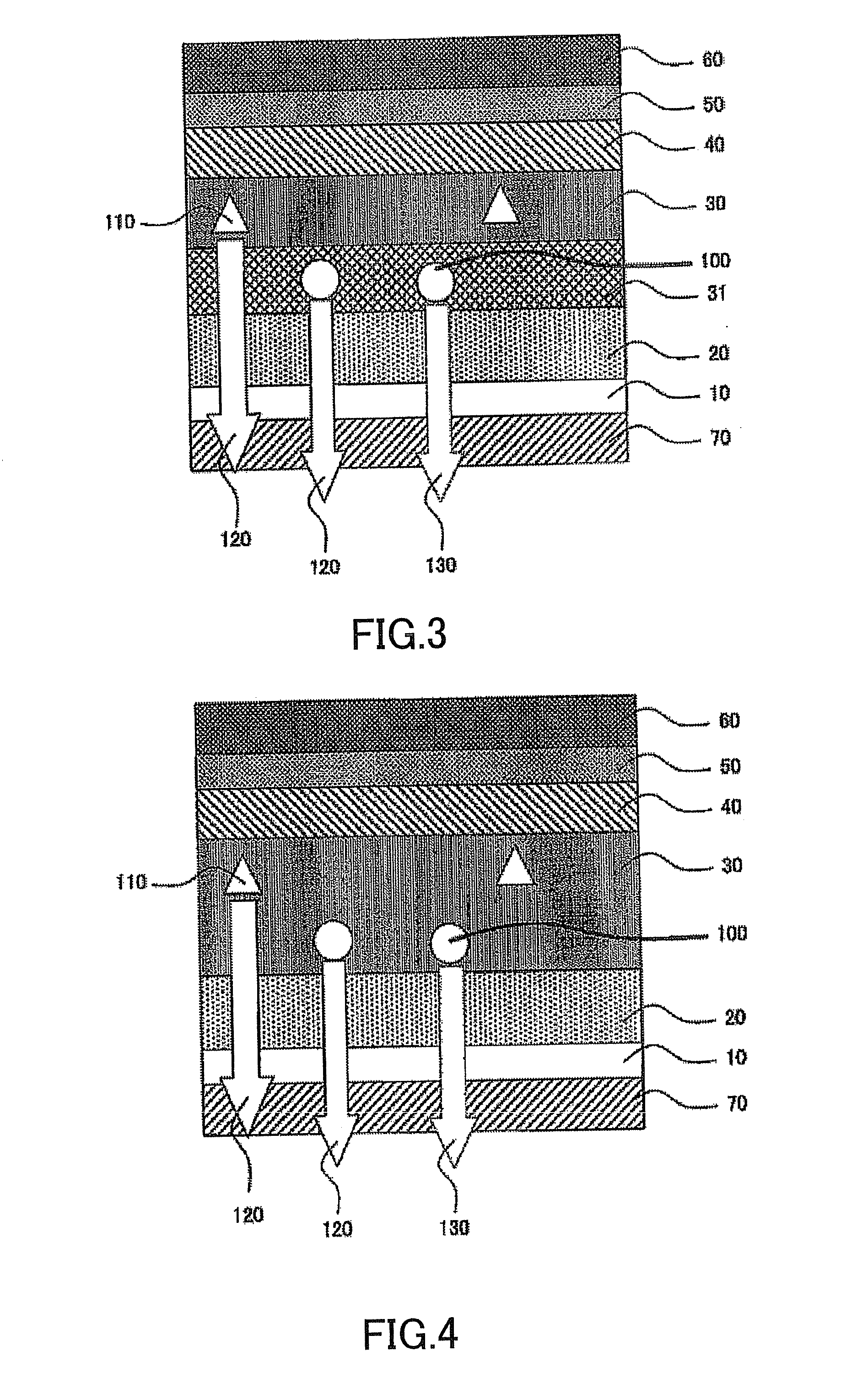
[0184]ITO / hole injection layer / hole transport layer / quantum dot-containing luminescent layer / hole block layer / electron transport layer / electron injection layer / cathode

[0185]A transparent anode, a hole injection layer, a hole transport layer, a quantum dot-containing luminescent layer, a hole block layer, an electron transport layer, an electron injection layer, and a cathode were formed and stacked in that order on a glass substrate, and the assembly was finally sealed to produce an organic EL device. All of works except for a transparent anode and a hole injection layer were carried out within a glove box of which the atmosphere was replaced by nitrogen (moisture concentration and oxygen concentration in glove box: not more than 0.1 ppm and not more than 0.1 ppm, respectively).

[0186]At the outset, a thin film (thickness: 150 nm) of indium tin oxide (ITO) was formed as a transparent anode. A glass substrate with ITO (manufactured by Sanyo Vacuum Industries Co., Ltd.) was patterned i...

example 2

[0191]An organic EL device of Example 2 was produced in the same manner as in Example 1 (amount of binder 1:amount of green light emitting QD having a protecting group 2 (weight ratio)=10:3), except that the green light emitting QD constituting the quantum dot-containing luminescent layer was prepared using a material having a protecting group 2 (luminescence wavelength 530 nm, dispersed in toluene) instead of the material having a protecting group 1.

example 3

[0192]An organic EL device of Example 3 was produced in the same manner as in Example 1 (amount of binder 1:amount of green light emitting QD having a protecting group 3 (weight ratio)=10:3), except that the green light emitting QD constituting the quantum dot-containing luminescent layer was prepared using a material having a protecting group 3 (luminescence wavelength 530 nm, dispersed in toluene) instead of the material having a protecting group 1.


PUM

PropertyMeasurementUnit
thicknessaaaaaaaaaa
luminescentaaaaaaaaaa
chemicalaaaaaaaaaa

Abstract

A QD protecting material having high compatibility with a binder component in a luminescent layer. The luminescent layer contains, as a part of its chemical structure, a compound containing a moiety A having a sum atomic weight MA of 100 or more and quantum dots protected by a protecting material, the protecting material contains, as a part of its chemical structure, a linking group connected to a quantum dot surface and a moiety B that has a sum atomic weight MB of 100 or more, satisfies a relationship between MB and MA represented by |MA−MB| / MB (2, and satisfies the requirement that the sum atomic weight MB is larger than one-third of the molecular weight of the protecting material, and a solubility parameter SA of the moiety A and a solubility parameter SB of the moiety B satisfy a relationship represented by |SA (SB| (2.

Description

CROSS-REFERENCE TO RELATED APPLICATIONS[0001]This application is based upon and claims the benefit of priority under Article 4 of the Paris Convention from the prior Japanese Patent Applications No. 256858 / 2007 filed on Sep. 28, 2007 and No. 249144 / 2008 filed on Sep. 26, 2008, the entire contents of the specifications, drawings, etc. of which are incorporated herein by reference.FIELD OF INVENTION[0002]The present invention relates to a light emitting device using quantum dots protected by a protecting material.BACKGROUND ART[0003]Light emitting devices are expected to be developed into a wide range of fundamental light emitting devices and applications, for example, organic electroluminescent devices (hereinafter referred to as organic EL device) and inorganic-organic hybrid light emitting devices.[0004]Organic EL devices are charge injection-type selfluminous devices utilizing luminescence produced upon recombination of electrons and holes arrived at the luminescent layer. Organic...

Claims


Application Information

Patent Timeline
Patent Type & Authority Applications(United States)
IPC IPC(8): H01L33/04
CPCH05B33/145H01L51/5012H10K50/11H05B33/14H05B33/20B82Y20/00H01L31/035218H10K50/115H10K85/115H10K85/151
Inventor OKADA, MASATOUENO, SHIGEHIROAKAI, TOMONORISHIMOGAWARA, MASAYATAKE, SEIJI
Owner DAI NIPPON PRINTING CO LTD
Why Eureka
Try Eureka