Manufacturing method of semiconductor laser element

Active Publication Date: 2010-09-23
HAMAMATSU PHOTONICS KK
View PDF7 Cites 116 Cited by
  • Summary
  • Abstract
  • Description
  • Claims
  • Application Information

AI Technical Summary

Benefits of technology

[0015]The present invention can improve the

Problems solved by technology

That is, if the object is initially subjected to both of the primary scribing and secondary scribing, the scratches formed by the secondary scrib

Method used


Image

  • Manufacturing method of semiconductor laser element
  • Manufacturing method of semiconductor laser element
  • Manufacturing method of semiconductor laser element

Examples


Embodiment Construction

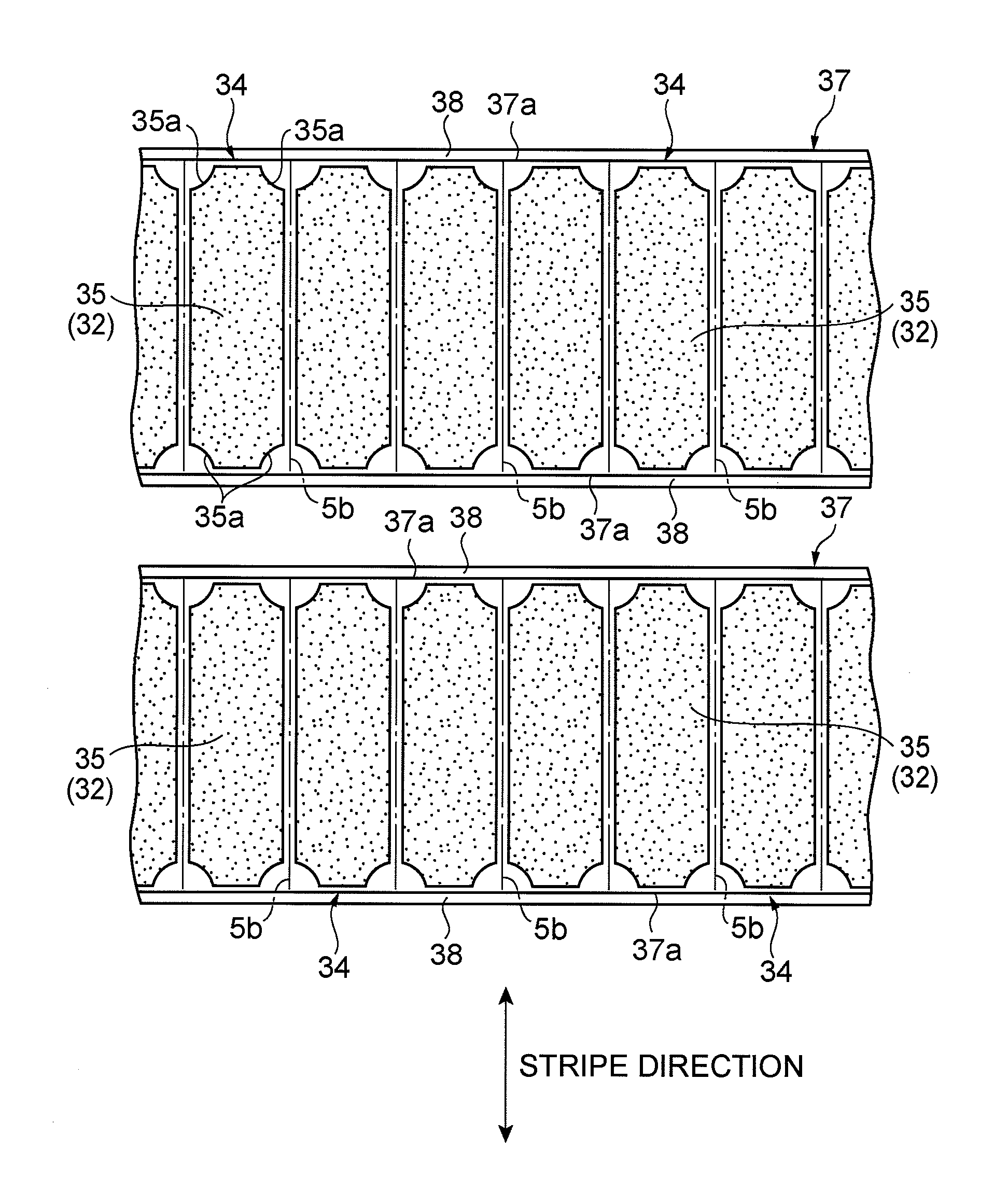
[0035]In the following, a preferred embodiment of the present invention will be explained in detail with reference to the drawings. In the drawings, the same or equivalent parts will be referred to with the same signs while omitting their overlapping explanations.

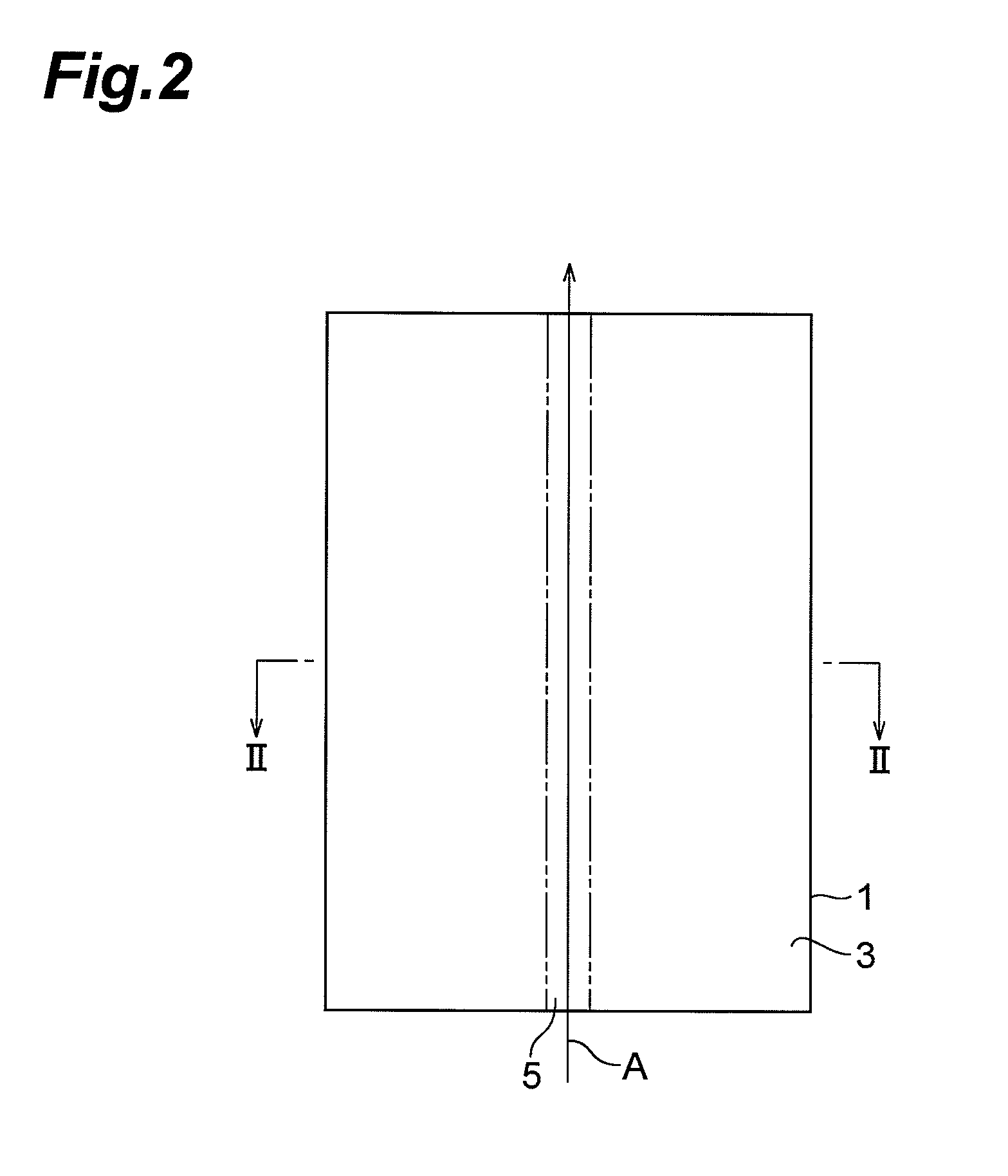
[0036]The method of manufacturing a semiconductor laser element in accordance with this embodiment irradiates a planar object to be processed with laser light while locating a converging point at the object, so as to form a modified region in the object along a line to cut the object.

[0037]Therefore, to begin with, the forming of a modified region in the method of manufacturing a semiconductor laser element in accordance with this embodiment will be explained with reference to FIGS. 1 to 9.

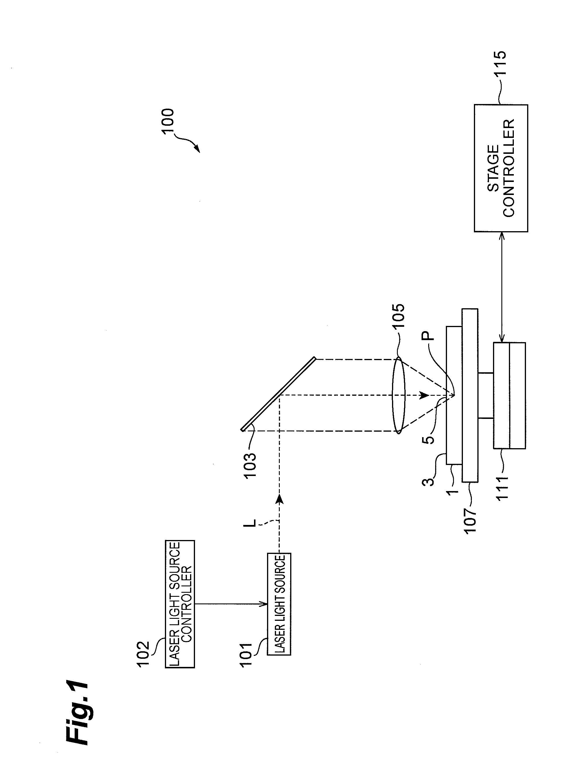
[0038]As illustrated in FIG. 1, a laser processing apparatus 100 comprises a laser light source 101 for pulsatingly oscillating laser light (processing laser light) L, a dichroic mirror 103 arranged such as to change the direction of the ...


PUM

PropertyMeasurementUnit
Forceaaaaaaaaaa

Abstract

Starting point regions for cutting 8a, 8b extending along lines to cut 5a, 5b are initially formed in an object to be processed 1. The starting point regions for cutting 8b have modified regions 7b formed by irradiating the object 1 with laser light while locating a converging point within the object 1 and are formed in parts extending along the lines to cut 5b excluding portions 34b intersecting the lines to cut 5a. This makes the starting point regions for cutting 8b much less influential when cutting the object 1 from the starting point regions for cutting 8a acting as a start point, whereby bars with precise cleavage surfaces can reliably be obtained. Therefore, it is unnecessary to form a starting point region for cutting along the lines to cut 5b in each of a plurality of bars, whereby the productivity of semiconductor laser elements can be improved.

Description

TECHNICAL FIELD[0001]The present invention relates to a method of manufacturing a semiconductor laser element having a stripe structure.BACKGROUND ART[0002]It has conventionally been typical for semiconductor laser elements having stripe structures to be manufactured as described in Non Patent Literature 1, for example.[0003]That is, an object to be processed in which a plurality of semiconductor laser parts to become semiconductor laser elements are arranged in a two-dimensional matrix is initially prepared. Then, the object is scratched with a scriber such as a diamond cutter along end parts of lines to cut extending orthogonal to a stripe direction between the semiconductor laser parts (primary scribing). Subsequently, the object is cleaved along the lines to cut from thus formed scratches acting as a start point, so as to yield a plurality of bars each having a plurality of semiconductor laser parts arranged one-dimensionally.[0004]Thereafter, the cleavage surfaces of the bars o...

Claims


Application Information

Patent Timeline
IPC IPC(8): H01L21/304B23K26/38B23K26/40B23K101/40H01L21/301H01S5/02
CPCB23K26/0057B23K26/0635B23K26/0853B23K26/4075H01S5/0201B28D5/0011C03B33/0222H01L21/78B23K2201/40B23K26/40B23K26/0624B23K26/53B23K2101/40B23K2103/50Y02P40/57
Inventor KUMAGAI, MASAYOSHIFUKUMITSU, KENSHIKUNO, KOJI
Owner HAMAMATSU PHOTONICS KK
Why Eureka
Try Eureka