Multi-Sacrificial Layer and Method

a technology of multi-sacrificial layer and micro-electromechanical system, which is applied in the field of multi-sacrificial layer and method, can solve the problems of large thermal budget, limited topography of the standard photoresist typically used as a sacrificial layer, and create defects in the mems structure, so as to reduce or eliminate variations

Active Publication Date: 2010-09-23
TAIWAN SEMICON MFG CO LTD
View PDF7 Cites 35 Cited by
  • Summary
  • Abstract
  • Description
  • Claims
  • Application Information

AI Technical Summary

Benefits of technology

[0011]An advantage of an embodiment of the present invention is the reduction or elimination of ...

Problems solved by technology

However, when using these processes the topography of the standard photoresist typically used as a sacrificial layer is limited by the fluid dynamic characteristics of the photoresist from forming a flat surface over the underlying features.
Such a non-planar surface can create problems during further processing of the device.
Not only may ...

Method used


Image

  • Multi-Sacrificial Layer and Method
  • Multi-Sacrificial Layer and Method
  • Multi-Sacrificial Layer and Method

Examples


Embodiment Construction

[0021]The making and using of embodiments of the present invention are discussed in detail below. It should be appreciated, however, that the present invention provides many applicable inventive concepts that can be embodied in a wide variety of specific contexts. The specific embodiments discussed are merely illustrative of specific ways to make and use the invention, and do not limit the scope of the invention.

[0022]The present invention will be described with respect to embodiments in a specific context, namely a multiple sacrificial layer structure for a variable capacitor MEMS device. The invention may also be applied, however, to other sacrificial structures and other types of devices.

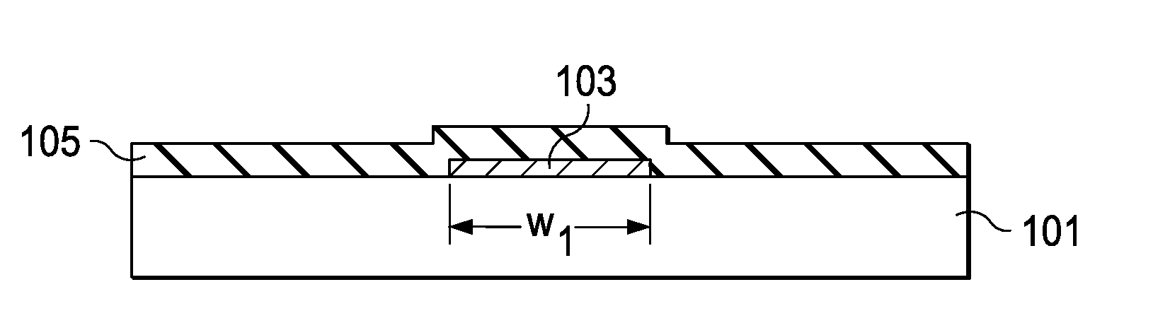
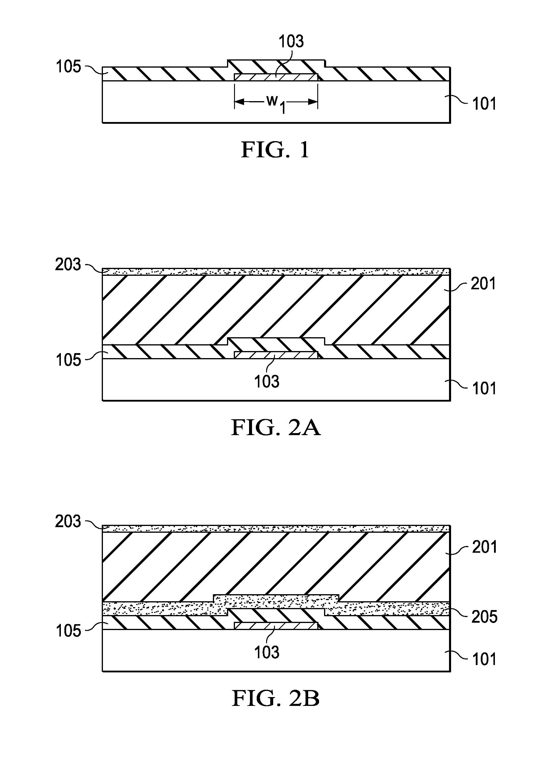
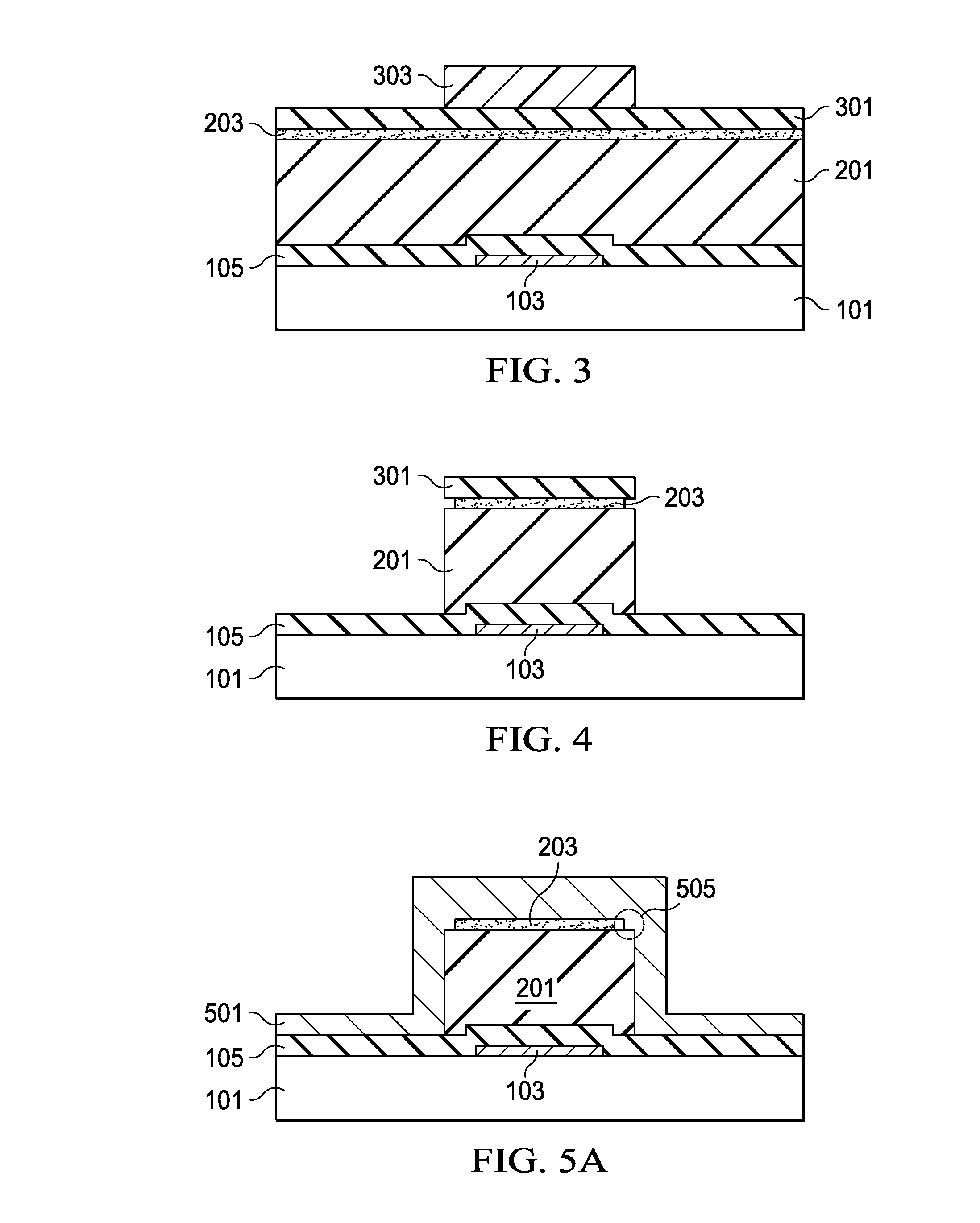
[0023]With reference now to FIG. 1, there is shown a substrate 101 with a variable capacitor bottom plate 103 and a dielectric layer 105 over the variable capacitor bottom plate 103. The substrate 101 may comprise bulk silicon, doped or undoped, or an active layer of a silicon-on-insulator (SOI) ...


PUM


Abstract

MEMS devices and methods for utilizing sacrificial layers are provided. An embodiment comprises forming a first sacrificial layer and a second sacrificial layer over a substrate, wherein the second sacrificial layer acts as an adhesion layer. Once formed, the first sacrificial layer and the second sacrificial layer are patterned such that the second sacrificial layer is undercut to form a step between the first sacrificial layer and the second sacrificial layer. A top capacitor electrode is formed over the second sacrificial layer, and the first sacrificial layer and the second sacrificial layer are removed in order to free the top capacitor electrode.

Description

[0001]This application claims the benefit of U.S. Provisional Patent Application Ser. No. 61 / 161,592, filed on Mar. 19, 2009, and entitled “Multi-Sacrificial Layer and Method,” which application is incorporated herein by reference.TECHNICAL FIELD[0002]The present invention relates generally to a microelectromechanical system devices and methods and, more particularly, to such devices and methods utilizing sacrificial layers.BACKGROUND[0003]Microelectromechanical system (MEMS) devices have been recently utilized in order to obtain devices with variable physical properties. Examples of these MEMS devices include devices with variable physical properties, such as digital micromirror devices (DMDs), and devices with variable electrical properties, such as variable capacitors or variable inductors. Generally, each of these MEMS devices comprises a moveable piece whose movement, when actuated by, e.g., an electrode, causes a change in the variable property of the device.[0004]Generally, w...

Claims


Application Information

Patent Timeline
IPC IPC(8): H01L21/28B05D1/32B05D5/12B05D3/14H01G9/00
CPCB81B2201/0221B81C1/0015H01L28/60H01G7/00H01G7/06B81C2201/0109
Inventor HUANG, YAO-TECHU, CHIA-HUAHSU, YU-NUCHENG, CHUN-WENPENG, LI-CHUNG
Owner TAIWAN SEMICON MFG CO LTD
Why Eureka
Try Eureka