Method of pattern etching a dielectric film while removing a mask layer

a dielectric film and mask layer technology, applied in the direction of electrical appliances, decorative surface effects, decorative arts, etc., can solve the problems of affecting the performance of the dielectric material, the interconnection delay is a major limitation factor, and the non-porous and porous low-k materials tend to be less robust than more traditional dielectric materials, and damag

Active Publication Date: 2010-09-30
TOKYO ELECTRON LTD
View PDF5 Cites 15 Cited by
  • Summary
  • Abstract
  • Description
  • Claims
  • Application Information

AI Technical Summary

Benefits of technology

[0006]The invention further relates to a method of pattern etching a thin film, and more particularly to a method for transferring a pattern to a thin film using a mask layer while substantially consuming the mask layer to avoid or reduce the need for a subsequent mask removal process.

Problems solved by technology

As is known to those in the semiconductor art, interconnect delay is a major limiting factor in the drive to improve the speed and performance of integrated circuits (ICs).
While low-k materials are promising for fabrication of semiconductor circuits, the present inventors have recognized that these films also provide many challenges.
Both non-porous and porous low-k materials tend to be less robust than more traditional dielectric materials and can be damaged during wafer processing, such as by etch and plasma ashing processes generally used in patterning the dielectric materials.

Method used


Image

  • Method of pattern etching a dielectric film while removing a mask layer
  • Method of pattern etching a dielectric film while removing a mask layer
  • Method of pattern etching a dielectric film while removing a mask layer

Examples


Embodiment Construction

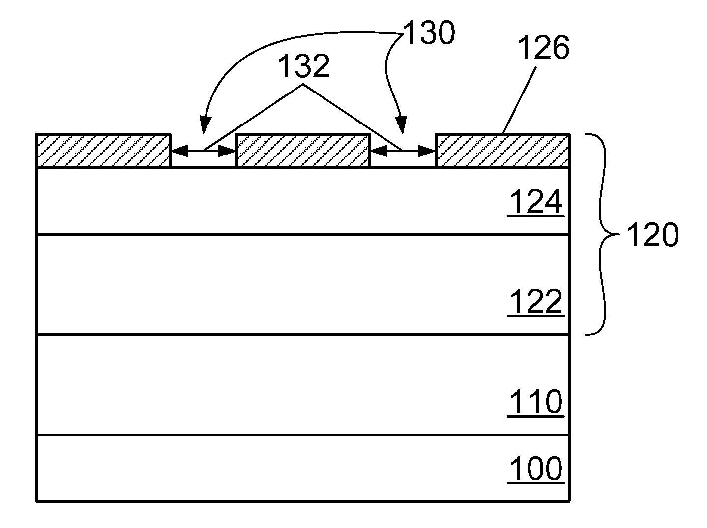
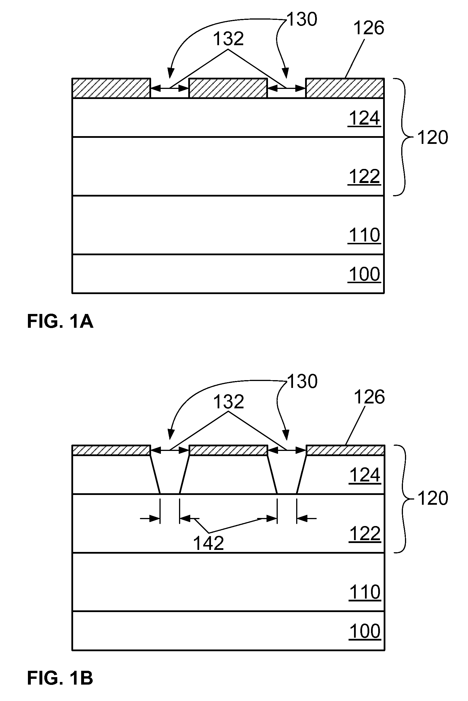
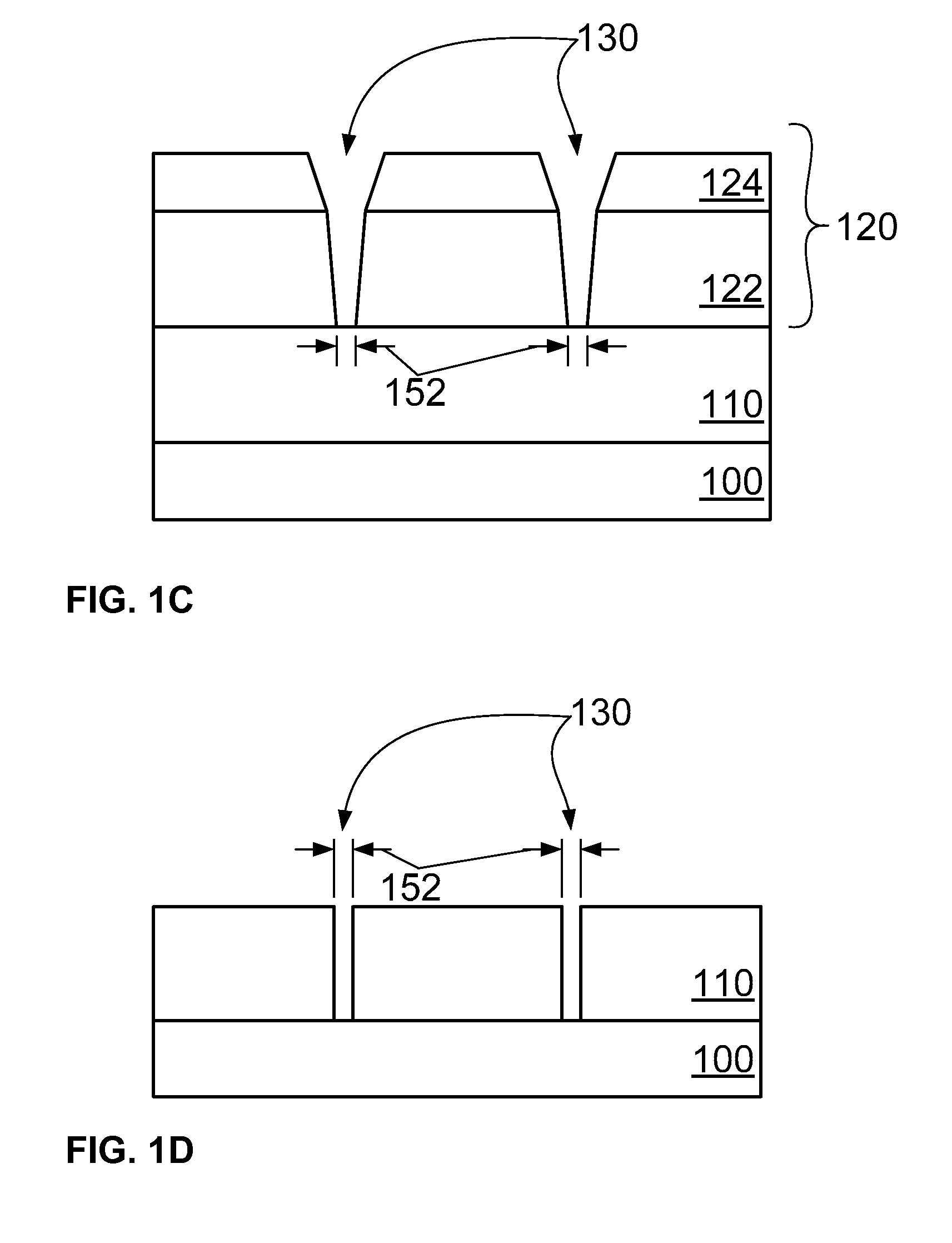
[0020]In the following description, for purposes of explanation and not limitation, specific details are set forth, such as a particular geometry of a processing system, descriptions of various components and processes used therein. However, it should be understood that the invention may be practiced in other embodiments that depart from these specific details.

[0021]Reference throughout this specification to “one embodiment” or “an embodiment” means that a particular feature, structure, material, or characteristic described in connection with the embodiment is included in at least one embodiment of the invention, but do not denote that they are present in every embodiment. Thus, the appearances of the phrases “in one embodiment” or “in an embodiment” in various places throughout this specification are not necessarily referring to the same embodiment of the invention. Furthermore, the particular features, structures, materials, or characteristics may be combined in any suitable manne...


PUM

PropertyMeasurementUnit
dielectric constantaaaaaaaaaa

Abstract

A method of pattern etching a thin film on a substrate is described. The method comprises preparing a film stack on a substrate, wherein the film stack comprises a dielectric layer formed on the substrate and a mask layer formed above the dielectric layer. A pattern is created in the mask layer, and the pattern is transferred from the mask layer to the dielectric layer by performing a plasma etching process. While transferring the pattern to the dielectric layer, the mask layer is substantially removed using the plasma etching process. The plasma etching process can use a process gas comprising a first gaseous component that etches the dielectric layer at a greater rate than the mask layer, and a second gaseous component that etches the dielectric layer at a lesser rate than the mask layer.

Description

BACKGROUND OF THE INVENTION[0001]1. Field of Invention[0002]The invention relates to a method of pattern etching a thin film, and more particularly to a method for transferring a pattern to a thin film using a mask layer while substantially consuming the mask layer to avoid a subsequent mask removal process.[0003]2. Description of Related Art[0004]As is known to those in the semiconductor art, interconnect delay is a major limiting factor in the drive to improve the speed and performance of integrated circuits (ICs). One way to minimize interconnect delay is to reduce interconnect capacitance by using low dielectric constant (low-k) materials during production of the ICs. Such low-k materials have also proven useful for low temperature processing. Thus, in recent years, low-k materials have been developed to replace relatively high dielectric constant insulating materials, such as silicon dioxide. In particular, low-k films are being utilized for inter-level and intra-level dielectr...

Claims


Application Information

Patent Timeline
Patent Type & Authority Applications(United States)
IPC IPC(8): B44C1/22
CPCH01L21/31116H01L21/31138H01L21/76816H01L21/67069H01L21/31144
Inventor LEE, YAO-SHENGBALASUBRAMANIAM, VAIDYANATHANNISHINO, MASARUZIN, KELVIN
Owner TOKYO ELECTRON LTD
Why Eureka
Try Eureka