

Method of manufacturing semiconductor package and semiconductor package
a manufacturing method and technology of semiconductors, applied in the direction of resist details, non-metallic protective coating applications, double resist layers, etc., to achieve the effect of enhancing the reliability of the semiconductor packag
- Summary
- Abstract
- Description
- Claims
- Application Information
AI Technical Summary
Benefits of technology
Problems solved by technology
Method used
Image

Examples
first embodiment
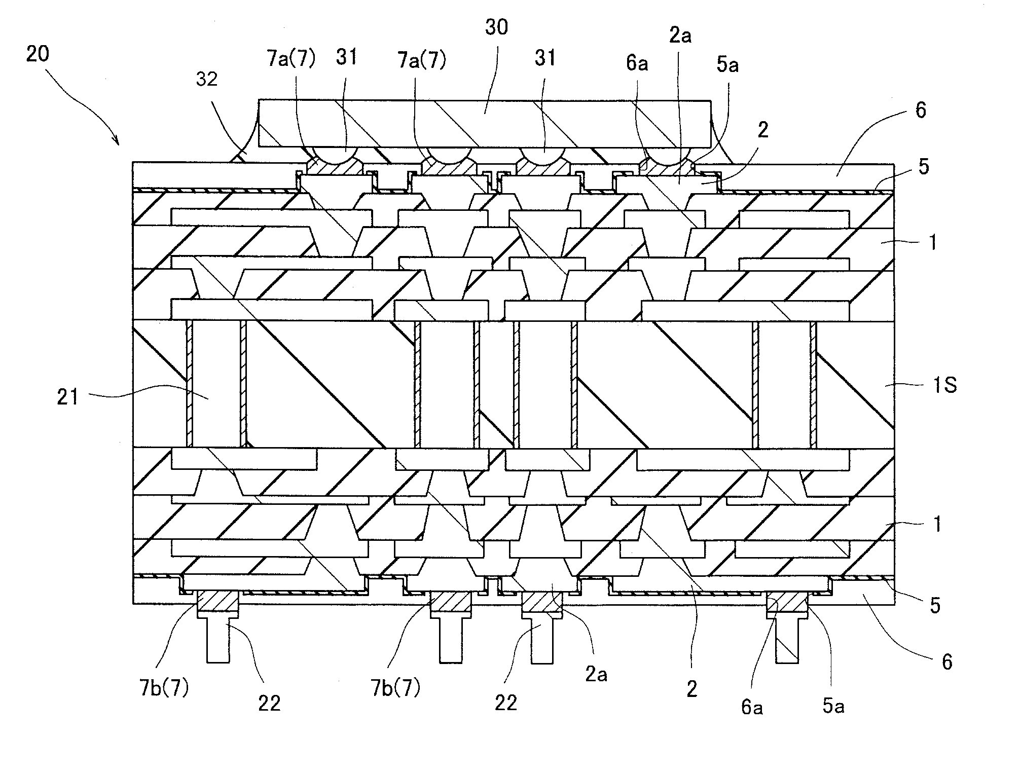
[0026]A method of manufacturing a semiconductor package according to the embodiment will be described with reference to FIGS. 1 to 6. As shown in FIG. 7, a semiconductor package 20 has, as a final configuration, a structure having a printed board (a board 1S) serving as a core, buildup resin layers 1 formed on both surfaces of the board 1S, and wirings 2 formed on the buildup resin layers 1, for example.
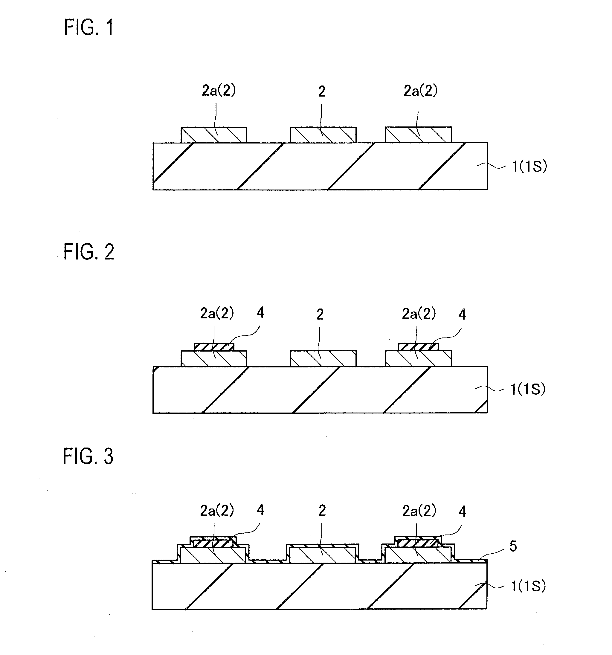
[0027]First of all, as shown in FIG. 1, there is prepared the board 1S on which the wiring 2 having an electrode pad 2a is formed. In FIG. 1, the buildup resin layer 1 formed as a top surface layer of the board 1S is indicated as the board 1S. The electrode pad 2a is formed integrally when a conductor film containing copper (Cu) as a principal component is subjected to patterning to form the wiring 2, for example. Moreover, an epoxy resin or a prepreg can be used for the buildup resin layer 1, for example, and the buildup resin layer 1 has an insulating property.
[0028]Next, the wirin...
second embodiment
[0051]A method of manufacturing a semiconductor package according to the embodiment will be described with reference to FIGS. 10 to 12. Overlapping description with the first embodiment will be omitted in some cases.
[0052]In the same manner as the step described with reference to FIG. 1, first of all, there is prepared a board 1S on which a wiring 2 having an electrode pad 2a is formed, and the wiring 2 including the electrode pad 2a is then subjected to a roughening treatment through a black oxidation treatment, a spraying treatment or a neobrown treatment, for example.
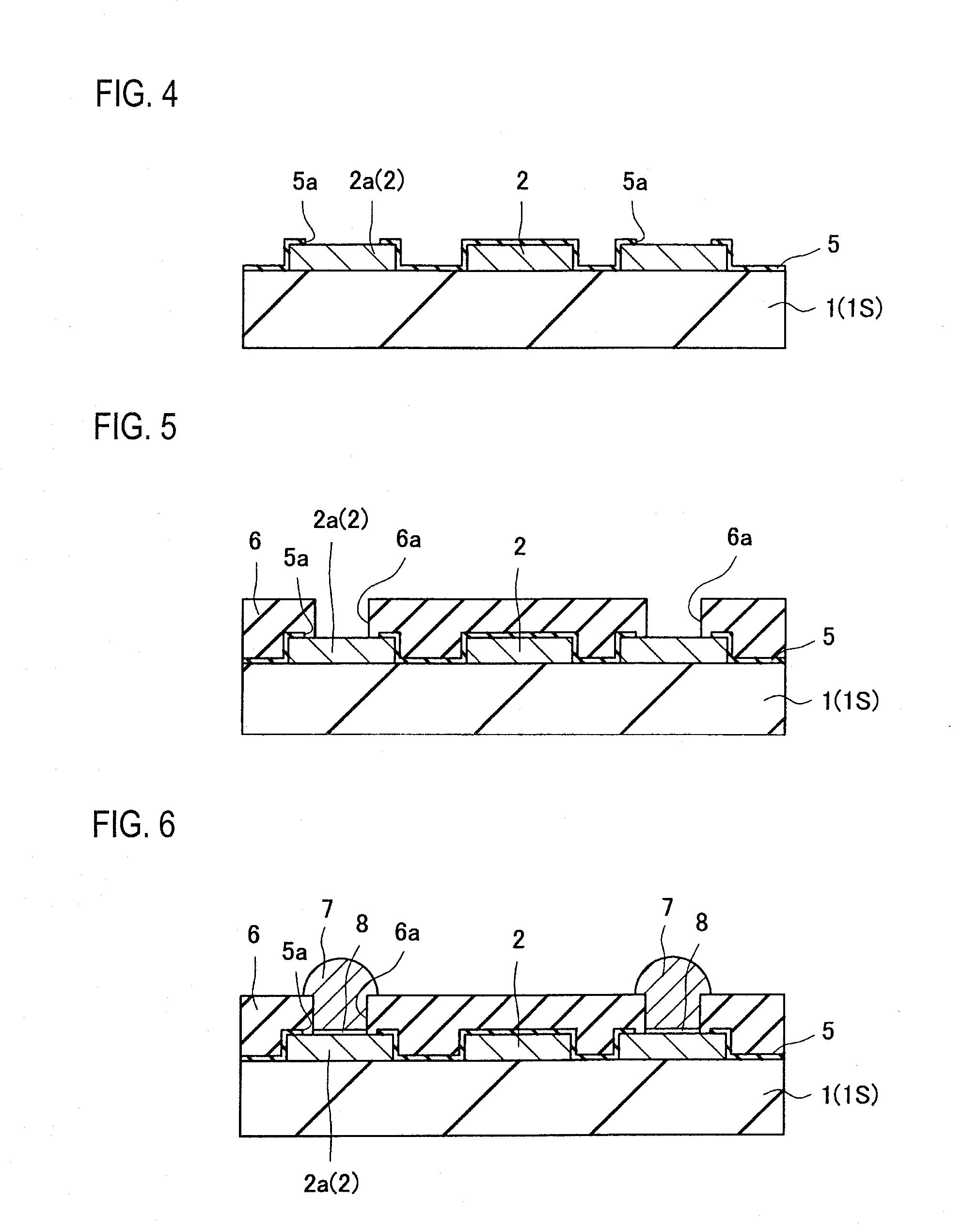
[0053]As shown in FIG. 10, subsequently, an inorganic insulating film 5 is formed on the board 1S in order to cover the wiring 2. The inorganic insulating film 5 is silicon oxide (for example, SiO2) with which a whole surface of the board 1S is coated by a plasma CVD method, for example.
[0054]Then, a solder resist layer 6 is formed on the board 1S in order to cover the inorganic insulating film 5. As shown in FIG. 11...
third embodiment
[0059]A method of manufacturing a semiconductor package according to the embodiment will be described with reference to FIGS. 13 to 15. Overlapping description with the first and second embodiments will be omitted in some cases.
[0060]In the same manner as the step described with reference to FIG. 1, first of all, there is prepared a board 1S on which a wiring 2 having an electrode pad 2a is formed, and the wiring 2 including the electrode pad 2a is then subjected to a roughening treatment through a black oxidation treatment, a spraying treatment or a neobrown treatment, for example.
[0061]In the same manner as the step described with reference to FIG. 10, subsequently, an inorganic insulating film 5 is formed on the board 1S in order to cover the wiring 2. The inorganic insulating film 5 is silicon oxide (for example, SiO2) with which a whole surface of the board 1S is coated by a plasma CVD method, for example.
[0062]Then, a resist film 9 is formed on the board 1S in order to cover t...
PUM
 Abstract
Description
Claims
Application Information