Unlock instant, AI-driven research and patent intelligence for your innovation.

Semiconductor device configuration method

a technology of semiconductor devices and configuration methods, applied in the field of configuration methods of semiconductor devices, can solve problems such as the increase of circuit area, and achieve the effect of reconfigurable wiring networks

Active Publication Date: 2010-09-30
NEC CORP
View PDF12 Cites 16 Cited by
  • Summary
  • Abstract
  • Description
  • Claims
  • Application Information

AI Technical Summary

Benefits of technology

[0027]As described above, in the present invention, a bus holder or a pull-up resistor for preventing floating is shared for configuration of the variable resistance switching elements to eliminate the need for adding extra MOS transistors, so that a reconfigurable wiring network can be realized in a small area without requiring MOS transistors for bypassing.

Problems solved by technology

The semiconductor device and configuration method as described above imply a problem that a circuit area increases.

Method used


Image

  • Semiconductor device configuration method
  • Semiconductor device configuration method
  • Semiconductor device configuration method

Examples


first embodiment

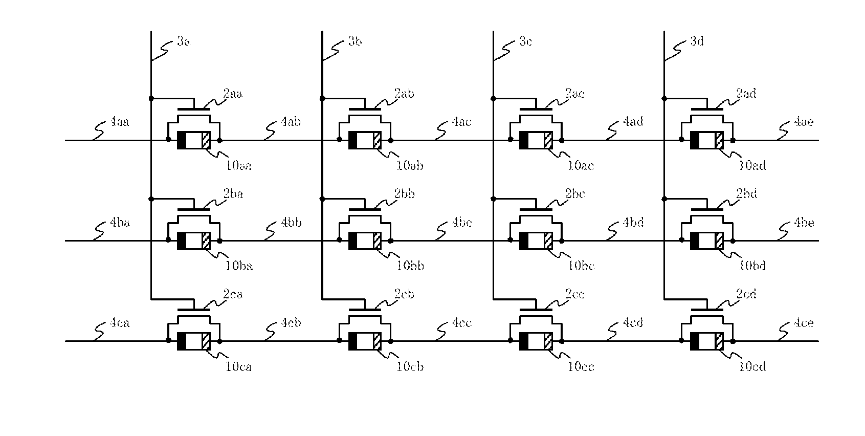
[0067]FIG. 4 is a diagram showing an exemplary configuration of a three-terminal variable resistance switching element for use in the present invention.

[0068]As shown in FIG. 4, three-terminal variable resistance switching element 11 comprises source electrode 20, drain electrode 21, ion conduction layer 22, and gate electrode 23.

[0069]Source electrode 20 is an electrode for supplying a metal ion, and is made, for example, of copper or the like. Drain electrode 21 is an electrode which does not supply a metal ion, and is made, for example, of platinum or the like. Ion conduction layer 22 is made, for example, of tantalum oxide. Gate electrode 23 is an electrode for supplying a metal ion, and is made of the same material as source electrode 20, for example, of copper or the like. Gate electrode 23 functions as a switch to bring source electrode 20 and drain electrode 21 into a conductive state or to put the electrodes into a shut-off state. Gate electrode 23 is provided for aiding in...

second embodiment

[0117]FIG. 12 is a diagram showing a second embodiment of a semiconductor device which comprises a reconfigurable wiring network using three-terminal variable resistance switching elements 11 shown in FIG. 4.

[0118]As shown in FIG. 12, this embodiment comprises pull-up resistor 6XY at voltage Vp, which is substituted for bus holder 5XY in the reconfigurable wiring network in the first embodiment shown in FIG. 6. In other words, in the second embodiment, pull-up resistor 6XY is comparable to the potential holding section described in the first embodiment.

[0119]The reconfigurable wiring network shown in FIG. 12 performs the same operation as the reconfigurable wiring network of the first embodiment described above. Specifically, the configuration method described in the first embodiment of the present invention can be applied as is to the reconfigurable wiring network in the second embodiment of the present invention. Pull-up resister 6XY at voltage Vp in the second embodiment of the p...


PUM


Abstract

A plurality of three-terminal variable resistance switching elements each having a source electrode, a drain electrode, and a gate electrode are connected to each other in series. The source electrode of each of the three-terminal variable resistance switching elements and the drain electrode of its adjacent three-terminal variable resistance switching element are connected to each other through a wiring segment to form a lane. A potential holding section for holding a predetermined potential level is connected to the wiring segment. A column group is configured by selecting one of the three-terminal variable resistance elements in each lane. A common gate line is connected to each of the gate electrodes of the three-terminal variable resistance elements belonging to the column group.

Description

TECHNICAL FIELD[0001]The present invention relates to a configuration method for a semiconductor device which comprises a reconfigurable wiring network using variable-resistance switching elements.BACKGROUND ART[0002]Recently developed switching elements (see, for example, JP2005-101535A) can be programmably set to a high-resistance state and a low-resistance state, can store the set state in a non-volatile manner, and can exhibit a significantly low on-resistance as compared with a MOS transistor having the same footprint area (hereinafter referred to as the “variable resistance switching element”).[0003]FIG. 1 is a diagram showing an exemplary configuration of a variable resistance switching element.[0004]Variable resistance switching element 10 shown in FIG. 1 comprises source electrode 20, drain electrode 21, and ion conduction layer 22. Source electrode 20 is an electrode for supplying a metal ion, and is made, for example, of copper or the like. Drain electrode 21 is an electr...

Claims


Application Information

Patent Timeline
IPC IPC(8): G11C11/00
CPCB82Y10/00G11C13/0011G11C13/003G11C13/0069G11C2013/009G11C2213/17H03K19/1778H01L27/101H01L27/24H03K19/17704H03K19/17736H03K19/17748G11C2213/75G11C2213/53H10B63/00
Inventor NAKAYA, SHOGO
Owner NEC CORP