Memory device, memory system having the same, and programming method of a memory cell

Inactive Publication Date: 2010-09-30
SAMSUNG ELECTRONICS CO LTD
View PDF25 Cites 14 Cited by
  • Summary
  • Abstract
  • Description
  • Claims
  • Application Information

AI Technical Summary

Benefits of technology

[0005]It is therefore a feature of an embodiment to provide a memory device that enables fast execution

Problems solved by technology

An entire block of resistive memory cells cannot be programmed or erased simultaneously, as t

Method used


Image

  • Memory device, memory system having the same, and programming method of a memory cell
  • Memory device, memory system having the same, and programming method of a memory cell
  • Memory device, memory system having the same, and programming method of a memory cell

Examples


Example

[0032]Korean Patent Application No. 10-2009-0025757, filed on Mar. 26, 2009, in the Korean Intellectual Property Office, and entitled: “Resistive memory device, memory system including same, and programming method of the same,” is incorporated by reference herein in its entirety.

[0033]Exemplary embodiments will now be described more fully hereinafter with reference to the accompanying drawings; however, they may be embodied in different forms and should not be construed as limited to the embodiments set forth herein. Rather, these embodiments are provided so that this disclosure will be thorough and complete, and will fully convey the scope of the invention to those skilled in the art. Like reference numerals refer to like elements / features throughout the specification.

[0034]Hereinafter, embodiments of the invention will be described using a phase change random access memory device (PRAM) example. However, it will be apparent to those skilled in the art that embodiments may be appli...


PUM


Abstract

A nonvolatile memory device having a plurality of multi-level memory cells, the plurality being at least two, may be programmed by writing a least significant bit for each multi-level memory cell of the plurality of memory cells and, after the least significant bit has been written for each multi-level memory cell of the plurality of memory cells, writing a next significant bit for each multi-level memory cell.

Description

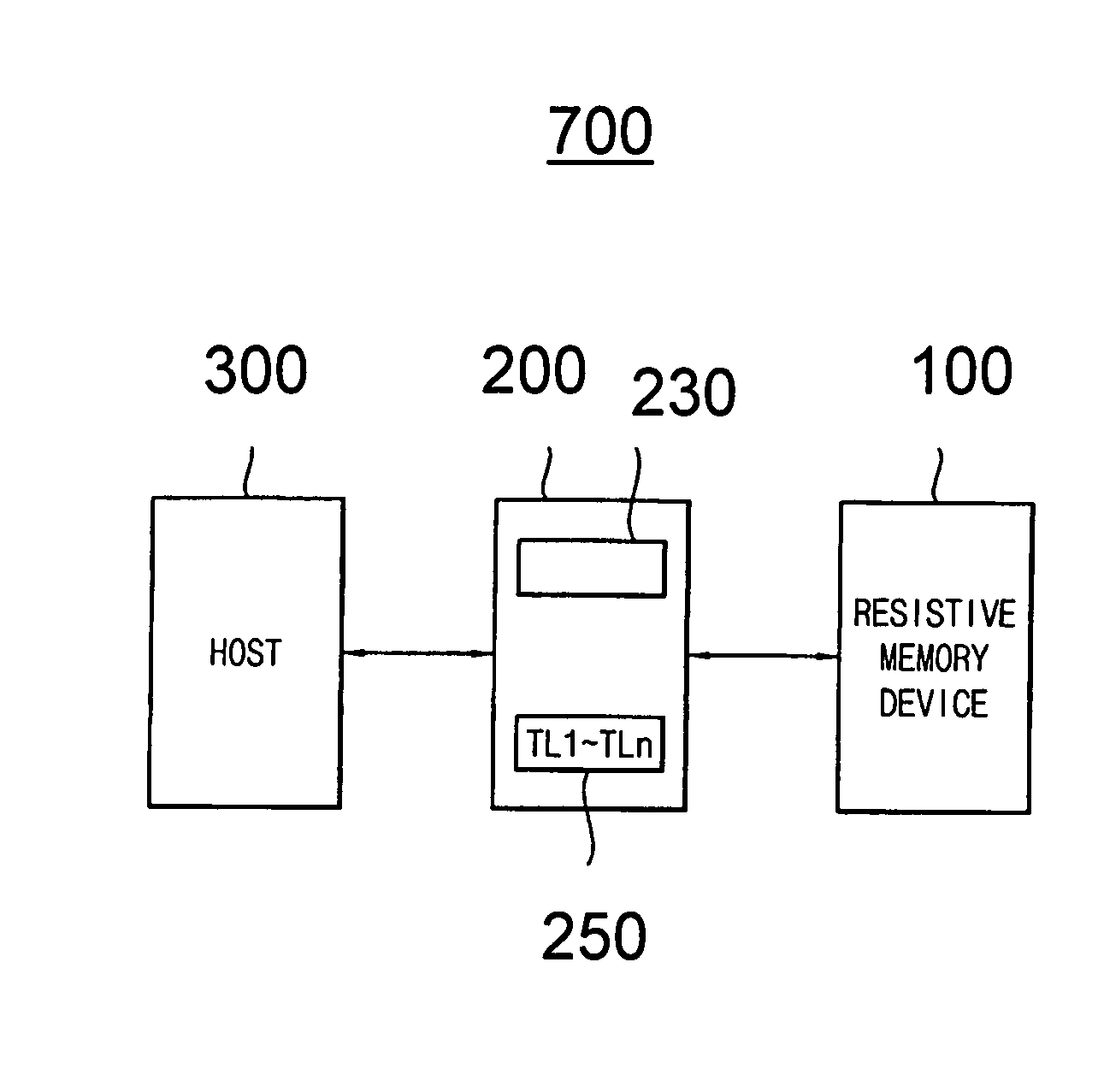
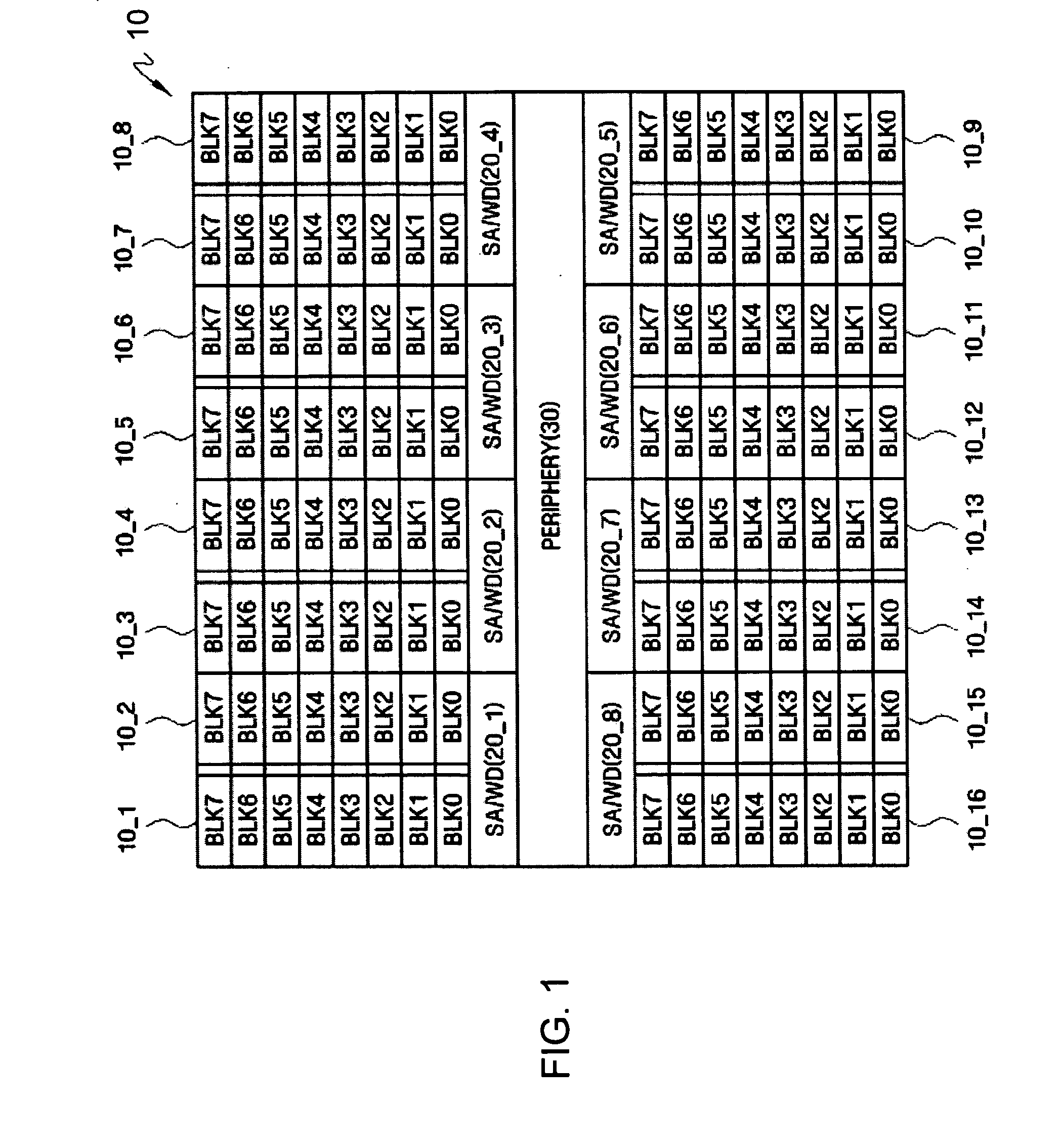
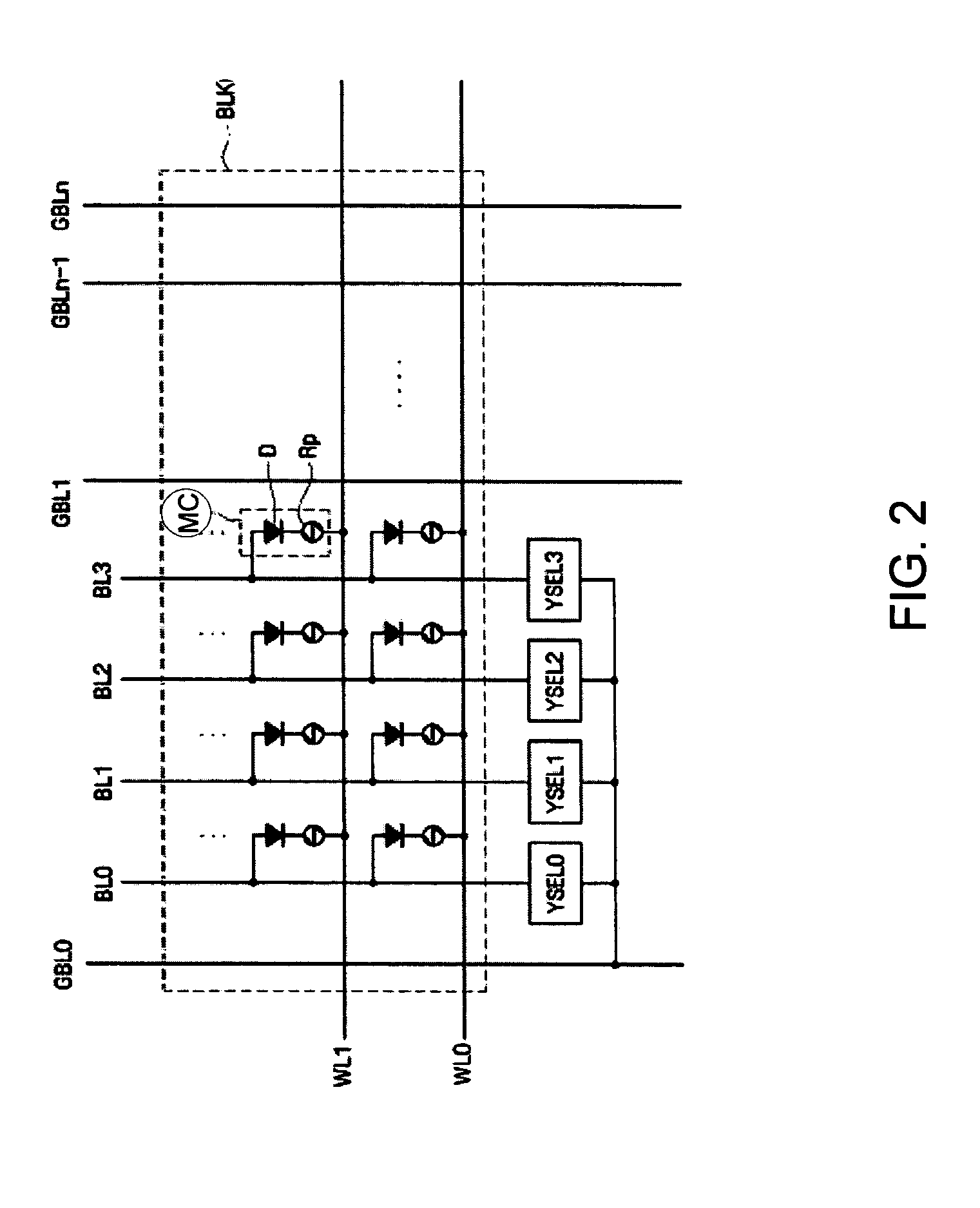
1. FIELD[0001]Embodiments relate to a semiconductor device, and more particularly, to a semiconductor device which enables fast execution of a program speed, a semiconductor system having the same, and a method of programming a memory cell.2. DESCRIPTION OF THE RELATED ART[0002]Memories are divided into volatile memories and non-volatile memories. Dynamic random access memories (DRAMs) and static random access memories (SRAMs) are volatile memories, while and flash memories, resistive memories, and phase change memories are non-volatile memories. The resistive memory uses a resistance value of a memory device to store one or more bits of data.[0003]An entire block of resistive memory cells cannot be programmed or erased simultaneously, as this would require too large a drive current. Accordingly, a block of such memory cells is programmed sequentially by applying a series of program pulses to respective cells. However, this results in a long programming time.SUMMARY[0004]Embodiments...

Claims


Application Information

Patent Timeline
IPC IPC(8): G11C11/00G06F12/00G06F12/06G11C7/00
CPCG06F12/0238G11C13/004G11C11/5678G11C11/5685G11C13/0004G11C13/0007G11C13/0069G11C2013/009G11C2211/5641G11C2211/5642G11C2211/5648G11C2213/32G11C2213/56G11C2213/72G11C2213/79G06F2212/7202
Inventor KIM, HO-JUNGKANG, SANG-BEOMPARK, CHUL WOOCHOI, HYUN HO
Owner SAMSUNG ELECTRONICS CO LTD
Why Eureka
Try Eureka