

Semiconductor element
a semiconductor element and semiconductor technology, applied in the field of semiconductor elements, can solve the problems of high production cost, limited materials which can be used as substrates, and high cost of cvd apparatuses used for the fabrication of tfts using silicon, so as to improve the electric characteristics of the semiconductor element, reduce the contact resistance, and low cost
- Summary
- Abstract
- Description
- Claims
- Application Information
AI Technical Summary
Problems solved by technology
Method used
Image

Examples
exemplary embodiment 1
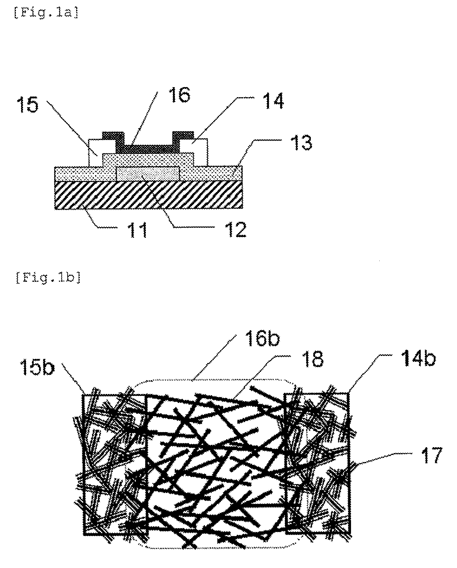
[0109]An example of the structure of a semiconductor element of the present invention is shown in FIG. 1. FIG. 1a is a schematic sectional view of a field-effect transistor which is a first exemplary embodiment of the present invention and in which a random network of CNTs is used for a channel layer. FIG. 1b is an enlarged plan view of parts of the channel layer and a source / drain electrode of the field-effect transistor.
[0110]A gate electrode 12 is formed on a supporting substrate 11. Further, a gate insulation film 13 is formed so as to cover the gate electrode 12. On the gate insulation film 13, a source electrode 14 and a drain electrode 15 are disposed at a distance corresponding to a channel length apart. Further, a random network of CNTs is disposed as a channel layer 16 so as to be in contact with the gate insulation film 13, the source electrode 14, and the drain electrode 15. The semiconductor element of the present invention is formed by the structure as described above....
exemplary embodiment 2
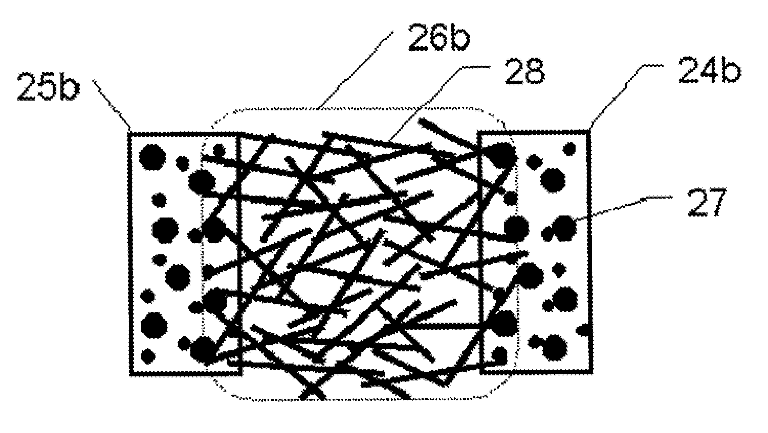
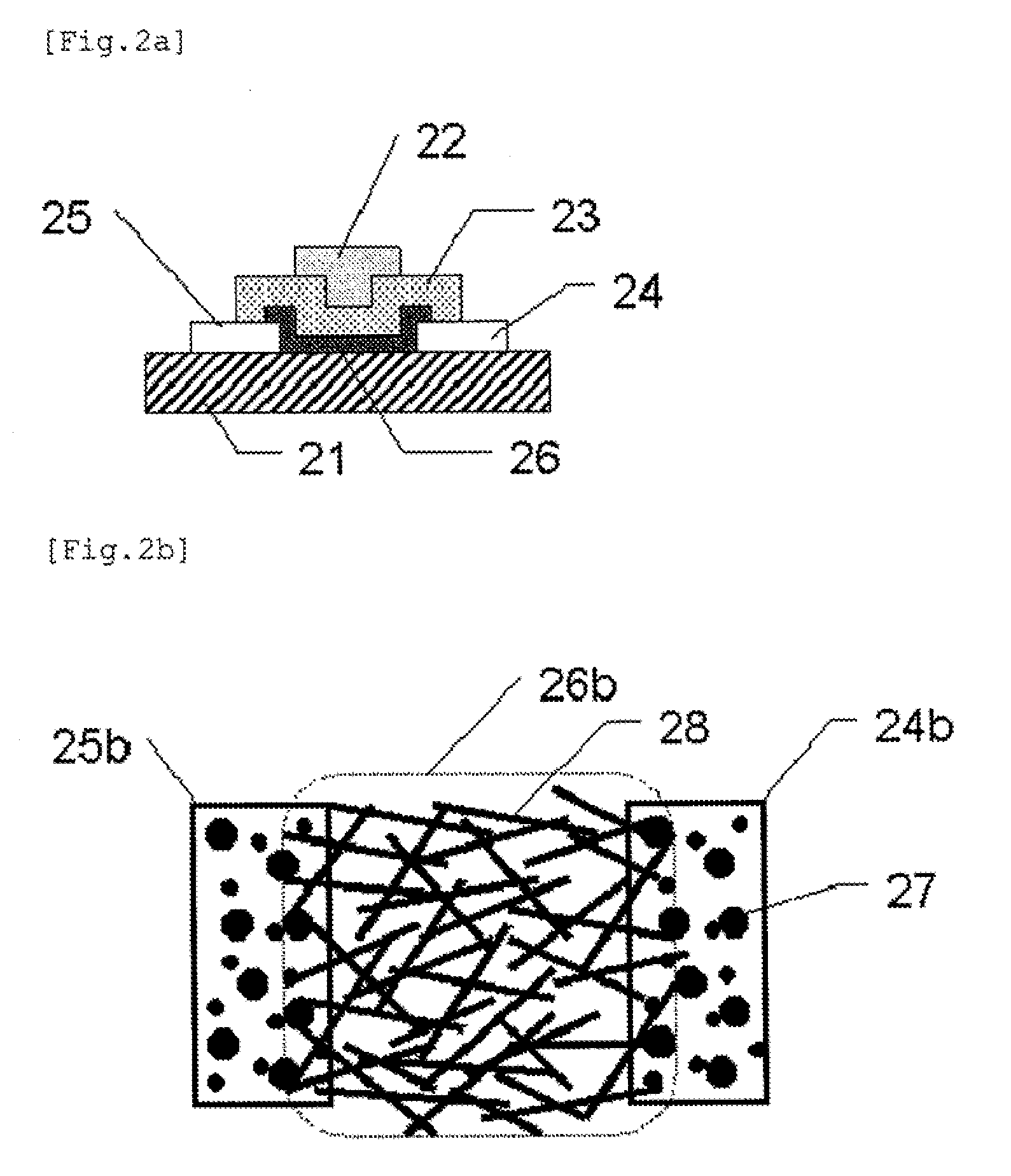
[0116]Further, a second example of the structure of the semiconductor element of the present invention is shown in FIG. 2. FIG. 2a is a schematic sectional view of a field-effect transistor which is a second exemplary embodiment of the present invention and in which a random network of CNTs is used for a channel layer. FIG. 2b is an enlarged plan view of parts of the channel layer and a source / drain electrode of a field-effect transistor.
[0117]A source electrode 24 and a drain electrode 25 are disposed at a distance corresponding to the channel length apart on a supporting substrate 21. A random network of CNTs is disposed as a channel layer 26 so as to be in contact with the source electrode 24 and the drain electrode 25. Further, a gate insulation film 23 is formed so as to cover the source electrode 24, the drain electrode 25, and the channel layer 26. Further, on top of that, a gate electrode 22 is formed. The semiconductor element of the second exemplary embodiment of the prese...
exemplary embodiment 3
[0123]An example of the structure of the semiconductor element of the present invention is shown in FIG. 3. FIG. 3a is a schematic sectional view to show a diode which is a third exemplary embodiment of the present invention and in which a random network of CNTs is used for the semiconductor layer. FIG. 3b is an enlarged plan view to show parts of the semiconductor layer and the electrodes of the diode.
[0124]A random network of CNTs is disposed as a semiconductor layer 36 on a supporting substrate 31. A first electrode 34 is disposed at one end of the semiconductor layer 36. A second electrode 35 is disposed at the other end of the semiconductor layer 36.
[0125]The region indicated by 34b of FIG. 3b, which is an enlarged plan view of the semiconductor element of the present invention, corresponds to the first electrode 34, and the region indicated by 35b corresponds to the second electrode 35. The first electrode 34b is formed by, for example, being drawn with an ink of silver nano-p...
PUM
| Property | Measurement | Unit |
|---|---|---|
| diameter | aaaaa | aaaaa |
| thickness | aaaaa | aaaaa |
| semiconductor | aaaaa | aaaaa |
Abstract
Description
Claims
Application Information