
Semiconductor device and manufacturing method for the same

a technology of semiconductors and manufacturing methods, applied in the direction of semiconductor devices, basic electric elements, electrical appliances, etc., can solve the problems of increasing source resistance, and achieve the effect of preventing the increase of source resistance and manufacturing methods

Inactive Publication Date: 2010-10-07
KK TOSHIBA
View PDF4 Cites 8 Cited by
  • Summary
  • Abstract
  • Description
  • Claims
  • Application Information

AI Technical Summary

Benefits of technology

The invention provides a semiconductor device that can prevent an increase in source resistance and a manufacturing method for the same. The semiconductor device includes a nitride based compound semiconductor layer, an active region, a gate electrode, a source electrode, a drain electrode, a gate terminal electrode, a source terminal electrode, a drain terminal electrode, and an end face electrode. The end face electrode has at least three metal layers and each of the three metal layers consisting of different metal. The semiconductor device can prevent an increase in source resistance and improve performance.

Problems solved by technology

For this reason, the semiconductor device having the end face electrode SC1, SC2, SC3, SC4 has a problem of causing increase of a source resistance.

Method used


Image

  • Semiconductor device and manufacturing method for the same
  • Semiconductor device and manufacturing method for the same
  • Semiconductor device and manufacturing method for the same

Examples


first embodiment

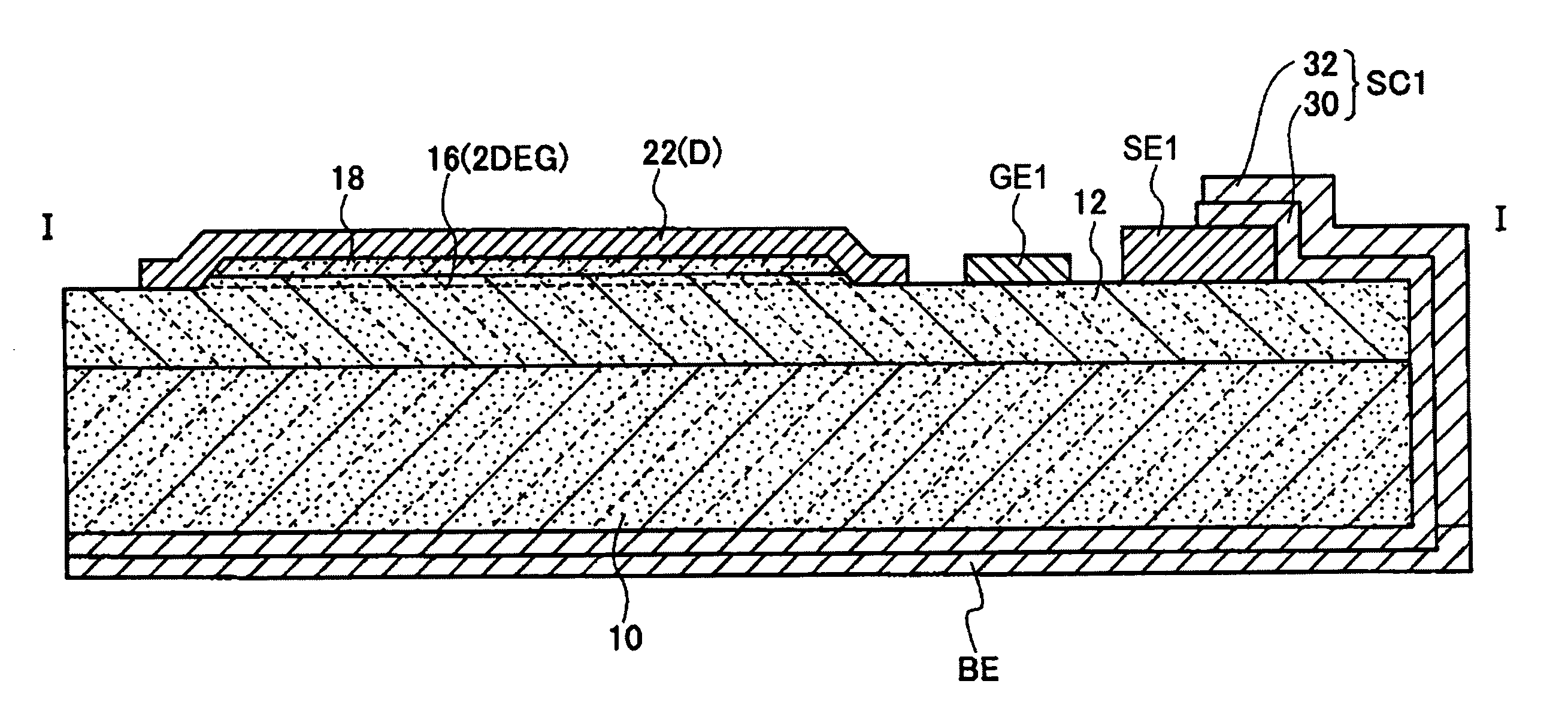
[0029](Device Structure)

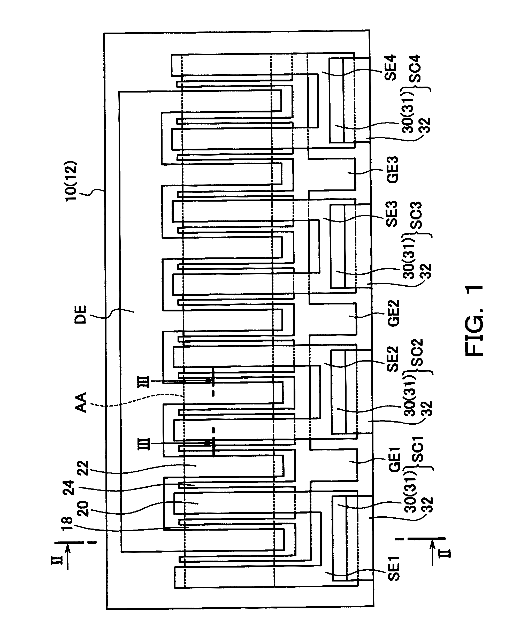
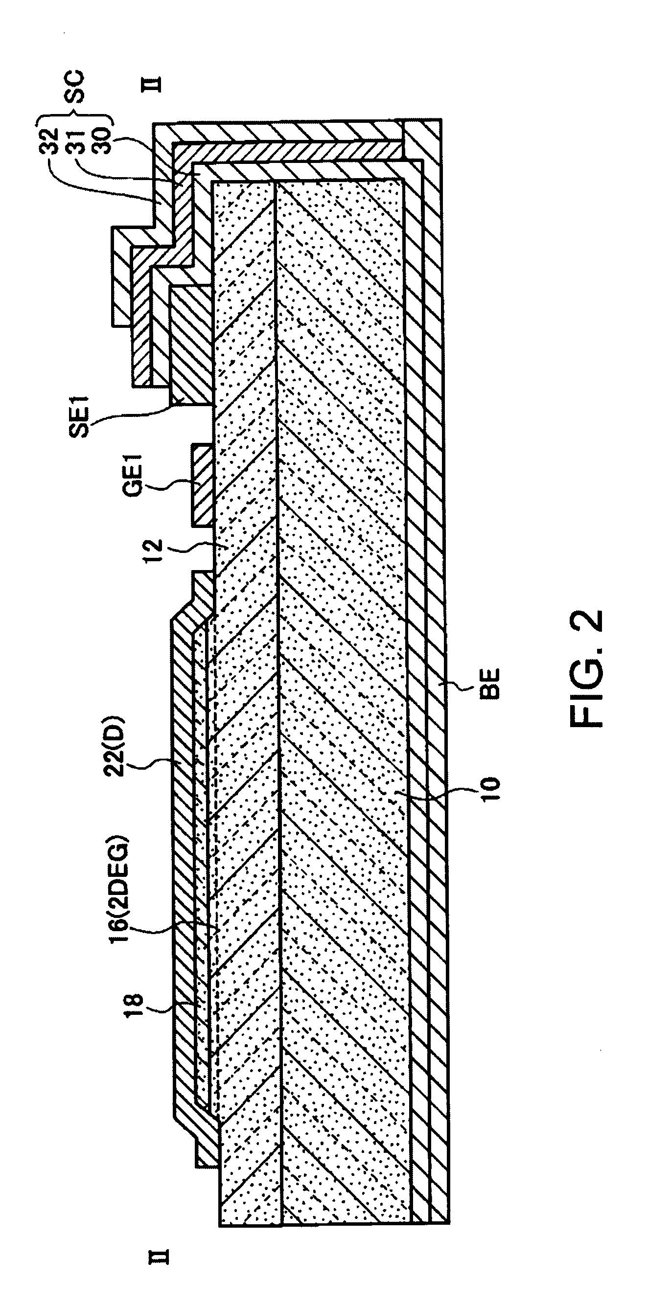
[0030]FIG. 1 shows a schematic plane pattern structure of a semiconductor device concerning the first embodiment of the invention. In addition, FIG. 2 shows a schematic cross sectional structure taken along a II-II line in FIG. 1.

[0031]As shown in FIGS. 1 and 2, the semiconductor device concerning the first embodiment has a substrate 10 which has SiC substrate, a nitride based compound semiconductor layer 12 arranged on the substrate 10, and an active region AA which has an aluminum gallium nitride layer (AlxGa1-xN) (0.1≦x≦1) 18 arranged on the nitride based compound semiconductor layer 12. The semiconductor device has a gate electrode 24, a source electrode 20, and a drain electrode 22 arranged on the active region AA. Further, the semiconductor device has gate terminal electrodes GE1, GE2, GE3 connected to the gate electrode 24, source terminal electrodes SE1, SE2, SE3, SE4 connected to the source electrode 20 and a drain terminal electrode DE connected to ...

example 1

Constitutional Example 1

[0045]As shown in FIG. 3, a semiconductor device has a substrate 10, a GaN epitaxial growth layer 12 arranged on the substrate 10, a aluminum gallium nitride layer (AlxGa1-xN) (0.1≦x≦1) 18 arranged on the GaN epitaxial growth layer 12, and a source electrode 20, a gate electrode 24 and a drain electrode 22 which have been arranged on the aluminum gallium nitride layer (AlxGa1-xN) (0.1≦x≦1) 18. A 2DEG layer 16 is formed in the interface between the GaN epitaxial growth layer 12 and the aluminum gallium nitride layer (AlxGa1-xN) (0.1≦x≦1) 18. In the semiconductor device shown in FIG. 3, an HEMT (High Electron Mobility Transistor) is configured.

example 2

Constitutional Example 2

[0046]Another constitutional example is shown in FIG. 4. A semiconductor device has a substrate 10, a GaN epitaxial growth layer 12 arranged on the substrate 10, a source region 26 and a drain area 28 formed in the GaN epitaxial growth layer 12, a source electrode 20 arranged on the source region 26, a gate electrode 24 arranged on the GaN epitaxial growth layer 12, and a drain electrode 22 arranged on the drain area 28.

[0047]In the semiconductor device shown in FIG. 4, an MESFET (Metal Semiconductor Field Effect Transistor) is configured.


PUM


Abstract

A semiconductor device which reduces source resistance and a manufacturing method for the same are provided. A semiconductor device has a nitride based compound semiconductor layer on a substrate and an active region on the nitride based compound semiconductor layer. The semiconductor device has a gate electrode, a source electrode and a drain on the active region, a source terminal electrode connected to the source electrode arranged on the nitride based compound semiconductor layer in a direction which the source electrode extends. Furthermore, the semiconductor device has an end face electrode which is arranged on the end face of the substrate in a source terminal electrode side, is connected to the source terminal electrode, and includes a multilayer metal layer including three or more layers which includes different metals, and prevents solder for die bonding from reaching the source terminal electrode.

Description

CROSS REFERENCE TO RELATED APPLICATION[0001]This application is based upon and claims the benefit of priority from the prior Japanese Patent Application No. 2009-93394, filed on Apr. 7, 2009, the entire contents of which are incorporated herein by reference.FIELD OF THE INVENTION[0002]The invention relates to a semiconductor device and a manufacturing method for the same, and relates especially to the semiconductor device which is capable of reducing a grounding inductance and operates in microwave band / millimeter wave band / submillimeter band, and the manufacturing method for the same.DESCRIPTION OF THE BACKGROUND[0003]An FET (Field Effect Transistor) using compound semiconductors, such as GaN (Gallium Nitride), has outstanding high frequency characteristics and is widely put in practical use as a semiconductor device which operates in microwave band / millimeter wave band / submillimeter wave band.[0004]A conventional semiconductor device is constituted as shown in FIGS. 11 and 12, for...

Claims


Application Information

Patent Timeline
Patent Type & Authority Applications(United States)
IPC IPC(8): H01L29/778H01L21/335
CPCH01L29/0692H01L29/2003H01L29/812H01L29/66462H01L29/7786H01L29/42316H01L29/41758
Inventor KAWASAKI, HISAO
Owner KK TOSHIBA
Learn More