Memory device and system including a memory device electronically connectable to a host circuit

a memory device and host circuit technology, applied in the direction of instruments, coding, code conversion, etc., can solve the problems of insufficient consideration of the dependability of communication communication faults may occur between the control unit provided, and the risk of problems such as errors arising in the memory contents of the memory device, so as to enhance communication reliability and improve the efficiency of reading and writing

Active Publication Date: 2010-10-07
SEIKO EPSON CORP
View PDF24 Cites 50 Cited by
  • Summary
  • Abstract
  • Description
  • Claims
  • Application Information

AI Technical Summary

Benefits of technology

[0009]An object of the present invention is to improve efficiency of reading and writing of actual data and error detection codes. Another object of

Problems solved by technology

However, in conventional techniques, insufficient consideration is given to the issue of dependability of communication between the control unit provided to the printer and the memory devices provided to the ink receptacles.
For example, there is a risk that, for reasons such as faulty contact between the electrical contact portions of the printer and an ink receptacle, communication faults may occur between the control unit provided to the printer and the memory device of the ink receptacle.
If operation of the print control unit is continued on wi

Method used


Image

  • Memory device and system including a memory device electronically connectable to a host circuit
  • Memory device and system including a memory device electronically connectable to a host circuit
  • Memory device and system including a memory device electronically connectable to a host circuit

Examples


modified embodiment 1

[0203]In the above embodiments, inverted data / Dn of the original data Dn is used as the related data for checking consistency with the original data Dn; however, other data having a prescribed logical relationship to the original data Dn may be used instead. As specific examples, related data such as the following may be used.

(1) A copy of the original data Dn

(2) Data resulting from addition of a prescribed value to the original data Dn

(3) Data resulting from subtraction of a prescribed value from the original data Dn

(4) Data resulting from multiplication of the original data Dn by a prescribed value

(5) Data resulting from a prescribed bit shift operation performed on the original data Dn

(6) Data resulting from a prescribed bit rotation operation performed on the original data Dn

[0204]Generally, it suffices for the original data Dn and the related data which is related to the original data Dn to have a prescribed logical relationship to one another, such that that the presence or l...

modified embodiment 2

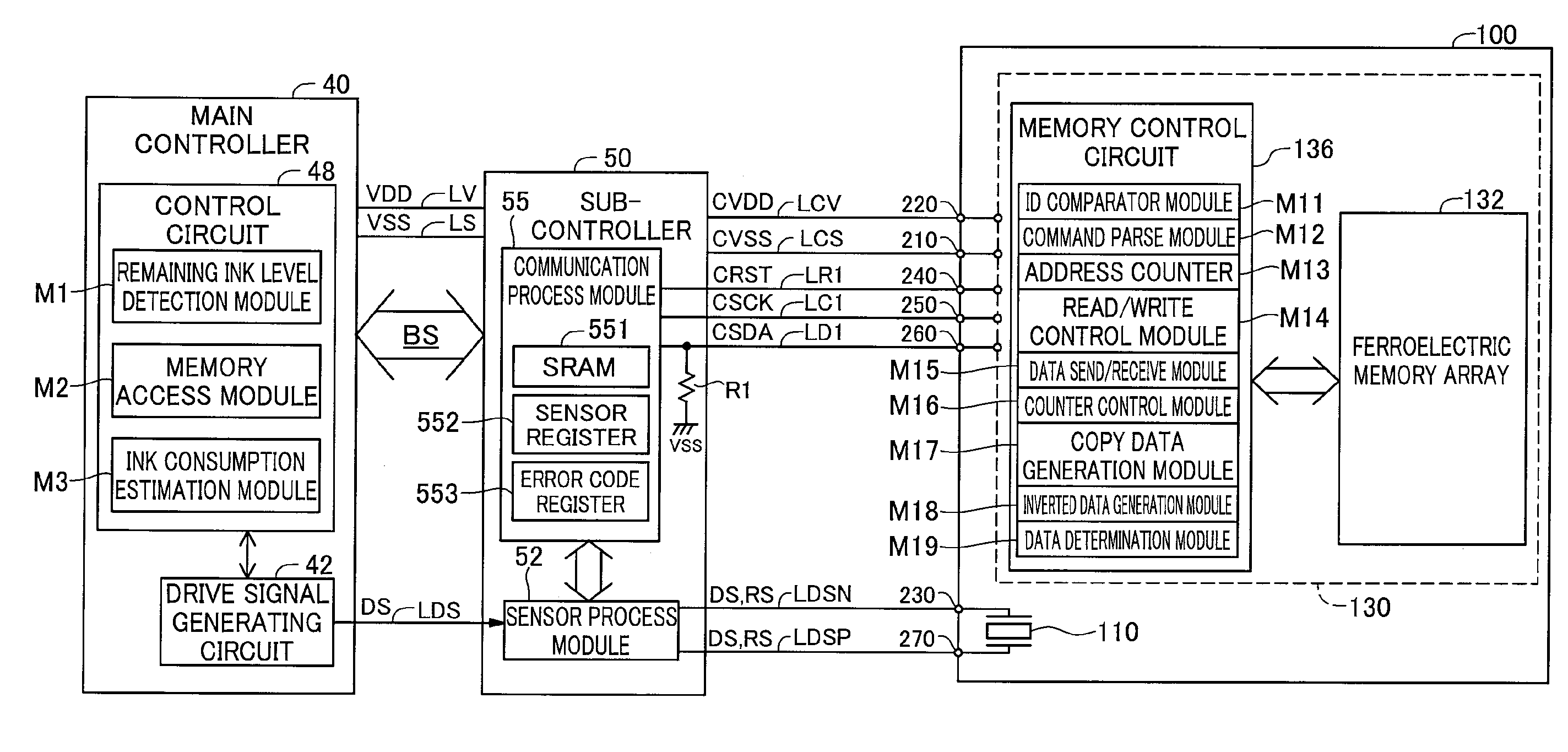
[0206]In the above embodiments, the memory cell array 132 is provided with both an original data area and a mirror data area; however, it is possible for the arrangement of data areas in the memory cell array 132 to be modified in various ways. For example, the memory cell array 132 may be provided with an original data area only. In this case, it is preferable for the memory control circuit 136 to be provided with a read copy data generation module adapted to copy data stored in the original data area and generate mirror data dn (copy data); and with an inverted data generation module adapted to invert each bit of the data stored in the original data area to generate inverted data / Dn and inverted mirror data / dn. Then, at the memory device 130, during the read operation the data send / receive module M15 of the memory control circuit 136 can send as the original data Dn the data that is stored in the original data area the sub-controller 50; and can send the mirror data dn, the inve...

modified embodiment 3

[0210]In the read operation in the above embodiments, original data Dn, inverted data / Dn, mirror data dn, and inverted mirror data / dn are sent from the memory device 130 to the sub-controller 50; however, there are various possible modifications with regard to the data that is sent during the read operation. For example, only the original data Dn and the inverted data / Dn may be sent, omitting sending of the mirror data dn and the inverted mirror data / dn. Alternatively, only the original data Dn and the mirror data dn may be sent, omitting sending of the inverted data / Dn and the inverted mirror data / dn.


PUM


Abstract

A memory includes a nonvolatile memory cell array, and a memory control circuit which carries out writing of data to and reading of data from the memory cell array in access units of N bits where N is an integer equal to 2 or greater. The memory cell array includes a rewritable area in which both writing of data and reading of data are permissible, and a read-only area in which writing of data is prohibited and reading of data is permissible. The rewritable area is configured so that the N bits constituting one access unit contain both actual data and an error detection code. The read-only area is divided between an actual data area in which the N bits constituting one access unit contain actual data, and an error detection code area in which the N bits constituting one access unit contain error detection codes.

Description

CROSS-REFERENCE TO RELATED APPLICATIONS[0001]The present application claims the priority based on Japanese Patent Applications No. 2009-088593 filed on Apr. 1, 2009, and No. 2009-195318 filed on Aug. 26, 2009, the disclosures of which are hereby incorporated by reference in their entireties.BACKGROUND OF THE INVENTION[0002]1. Field of the Invention[0003]The present invention relates to a memory device, and to a system including a memory device electrically connectable to a host circuit.[0004]2. Description of the Related Art[0005]An inkjet printer, which is one example of liquid ejecting apparatus, typically has one or more installed ink receptacles provided as detachable liquid receptacles. Some ink receptacles are furnished with memory devices. The memory device stores information of various kinds, for example, the remaining ink level or the color of the ink in the ink receptacle (see JP 2002-370383 A, JP 2004-299405 A). A control unit provided to the printer communicates with the...

Claims


Application Information

Patent Timeline
IPC IPC(8): G06F11/07G06F12/16
CPCG06F11/1008B41J2/17546
Inventor KOSUGI, YASUHIKO
Owner SEIKO EPSON CORP
Why Eureka
Try Eureka