Thin film semiconductor device, display device using such thin film semiconductor device and manufacturing method thereof
a thin film semiconductor and display device technology, applied in the direction of optics, identification means, instruments, etc., can solve the problems of reducing manufacturing costs, unable to achieve the optimal energy for laser irradiation to acquire large carrier mobility, and unable to achieve laser irradiation with the optimum energy to achieve large carrier mobility, the effect of reducing the thermal capacity of the semiconductor devi
- Summary
- Abstract
- Description
- Claims
- Application Information
AI Technical Summary
Benefits of technology
Problems solved by technology
Method used
Image

Examples
Embodiment Construction
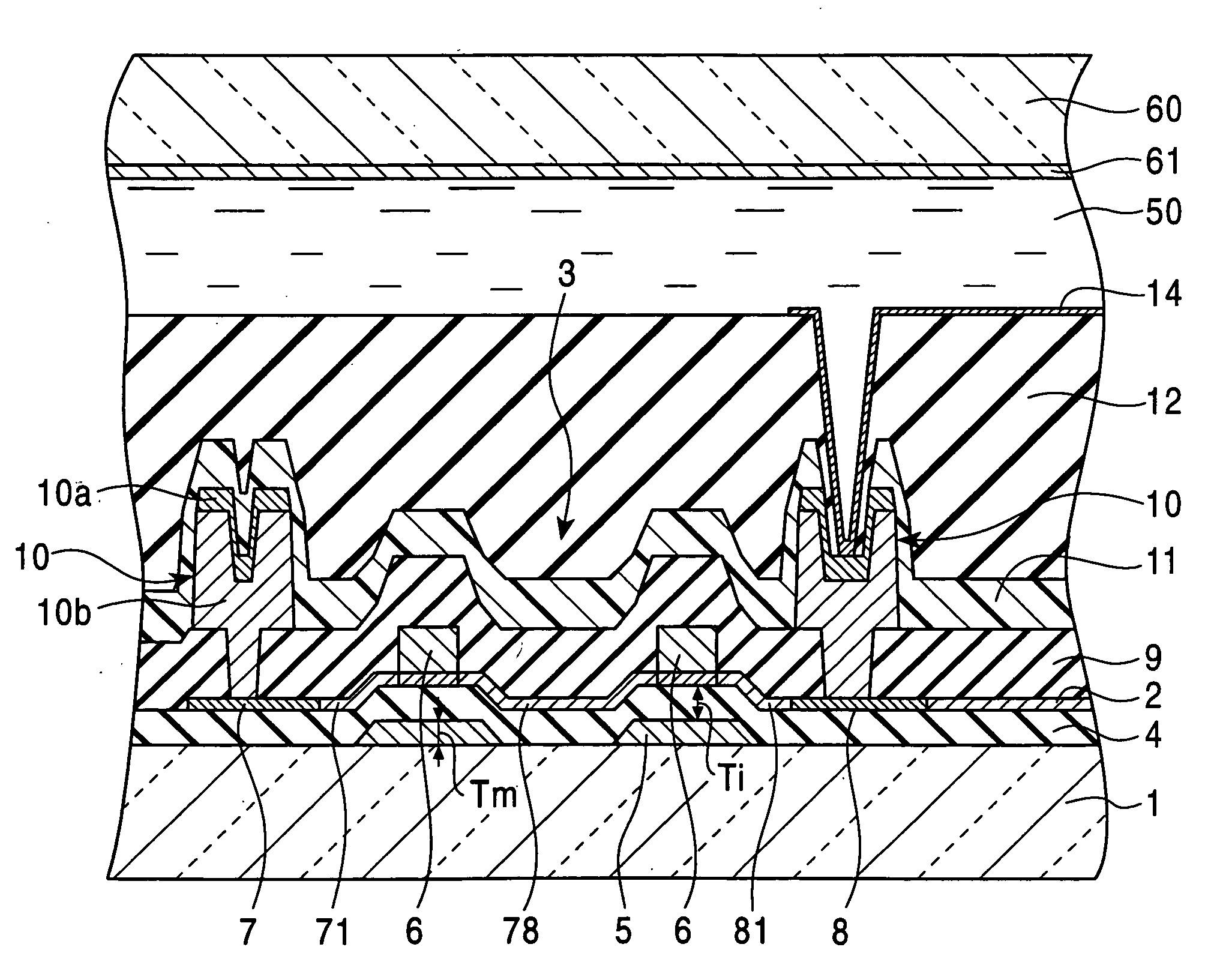
[0034]Referring to the following drawings, embodiments of this invention are described in detail. FIG. 1 illustrates one example of a partially sectional view in schematic form showing a first embodiment of a thin film semiconductor device relating to this invention. As illustrated, this thin film semiconductor device is such that a bottom gate structured thin film transistors 3 stacked with a gate electrodes 5, a gate insulating film 4 and a semiconductor thin film 2 in the order from below upward is formed as integrated circuits on an insulating substrate 1 such as glass or the like. This thin film semiconductor device is used as a driving substrate for an active matrix typed display device. For this purpose, pixel electrodes 14 are connected with the thin film transistors 3. In addition, the thin film transistors 3 employ a double gate structure to enhance reliability. However, this invention is not limited to the double gate structure. It is needless to say that this invention i...
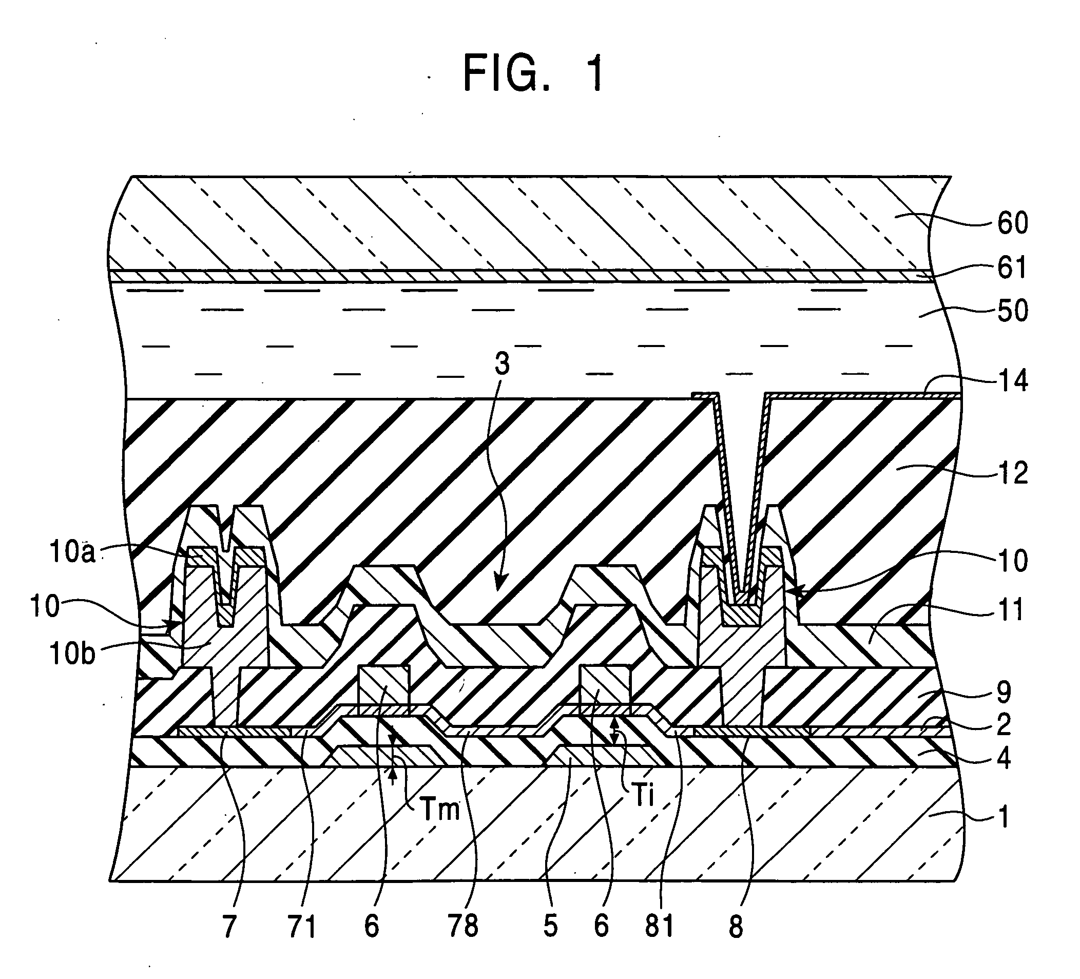
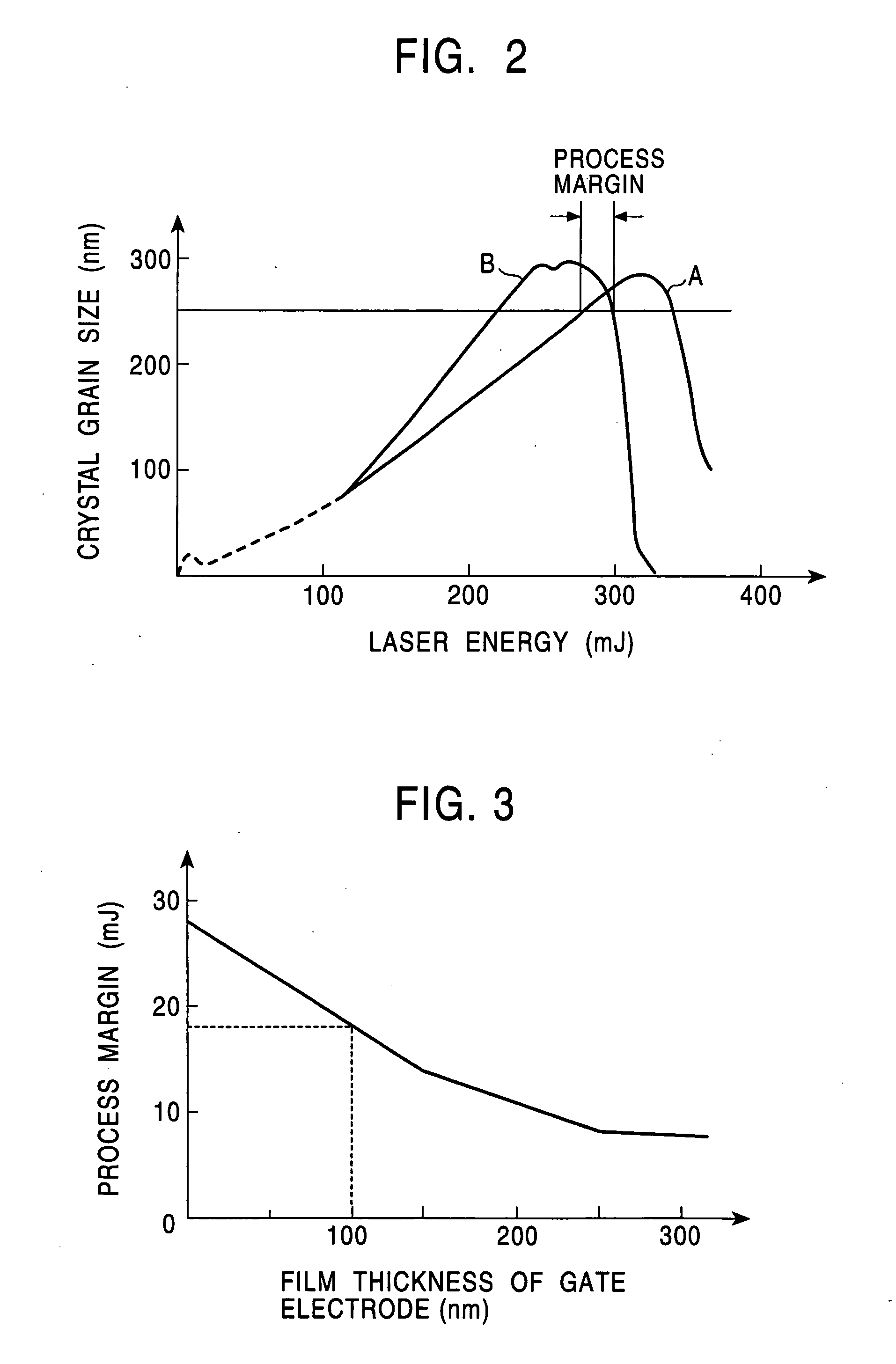
PUM
| Property | Measurement | Unit |
|---|---|---|
| thickness | aaaaa | aaaaa |
| crystal grain sizes | aaaaa | aaaaa |
| temperature | aaaaa | aaaaa |
Abstract
Description
Claims
Application Information
 - R&D Engineer
- R&D Manager
- IP Professional
- Industry Leading Data Capabilities
- Powerful AI technology
- Patent DNA Extraction
Browse by: Latest US Patents, China's latest patents, Technical Efficacy Thesaurus, Application Domain, Technology Topic.
© 2024 PatSnap. All rights reserved.Legal|Privacy policy|Modern Slavery Act Transparency Statement|Sitemap