Semiconductor device

a technology of semiconductor devices and semiconductors, applied in semiconductor devices, semiconductor/solid-state device details, electrical apparatus, etc., can solve the problems of inability to follow electric signals, difficult to reduce the size of each photo coupler, and signal attenuation, so as to maximize the efficiency of signal transmission from the first circuit to the second circuit

Active Publication Date: 2010-10-21
RENESAS ELECTRONICS CORP
View PDF3 Cites 21 Cited by
  • Summary
  • Abstract
  • Description
  • Claims
  • Application Information

AI Technical Summary

Benefits of technology

[0021]According to the embodiment, the distance from the first inductor to the third inductor differs from the distance from the second inductor to the fourth inductor. The breakdown voltage between the first circuit and the second circuit is determined by the sum of the distance from the first inductor to the third inductor and the distance from the second inductor to the fourth inductor. Therefore, the sum of the distance from the first inductor to the third inductor and the distance from the second inductor to the fourth inductor needs to be equal to or larger than a certain value. When a semiconductor ...

Problems solved by technology

However, it is difficult to reduce the size of each photo coupler due to the existence of the light emitting element and the light receiving element.
Also, where the frequency of electric signals is high, the photo couplers cannot follow the electric signals.
Therefore, there is a possibility that signal attenuation occurs while signals are being transferred, and the signals cannot be transferred accurately.
However, where the reference voltage of the transmission-si...

Method used


Image

  • Semiconductor device
  • Semiconductor device
  • Semiconductor device

Examples


first embodiment

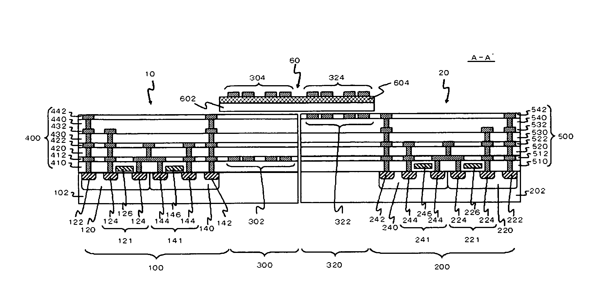
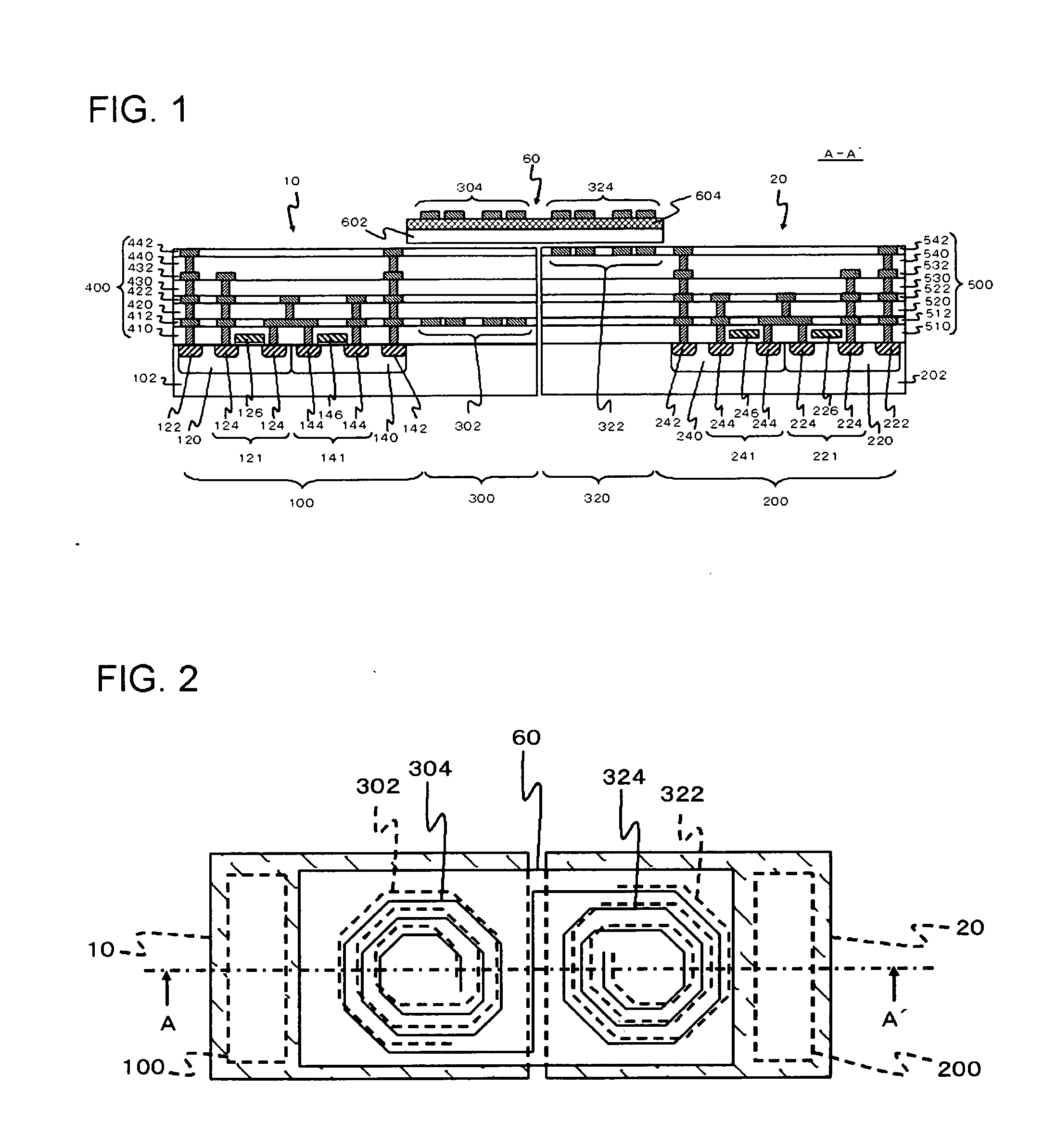
[0036]FIG. 1 is a diagram showing the structure of a semiconductor device according to a first embodiment. FIG. 2 is a schematic plan view of the semiconductor device shown in FIG. 1. FIG. 1 is a cross-sectional view of the semiconductor device, taken along the line A-A′ of FIG. 2. For simplification of the drawings, the number of windings in each of the later described first inductor 302 and second inductor 322 in FIG. 1 differs from the number of windings shown in FIG. 2. This semiconductor device includes two semiconductor chips 10 and 20, and an interconnect substrate 60. The semiconductor chip 10 includes a multilayer interconnect 400, and the semiconductor chip 20 includes a multilayer interconnect 500.

[0037]The semiconductor chip 10 includes a first substrate 102, a first circuit 100, and a first inductor 302. The first substrate 102 is a semiconductor substrate such as a silicon substrate. The first circuit 100 generates signals to be transmitted. The first inductor 302 is f...

second embodiment

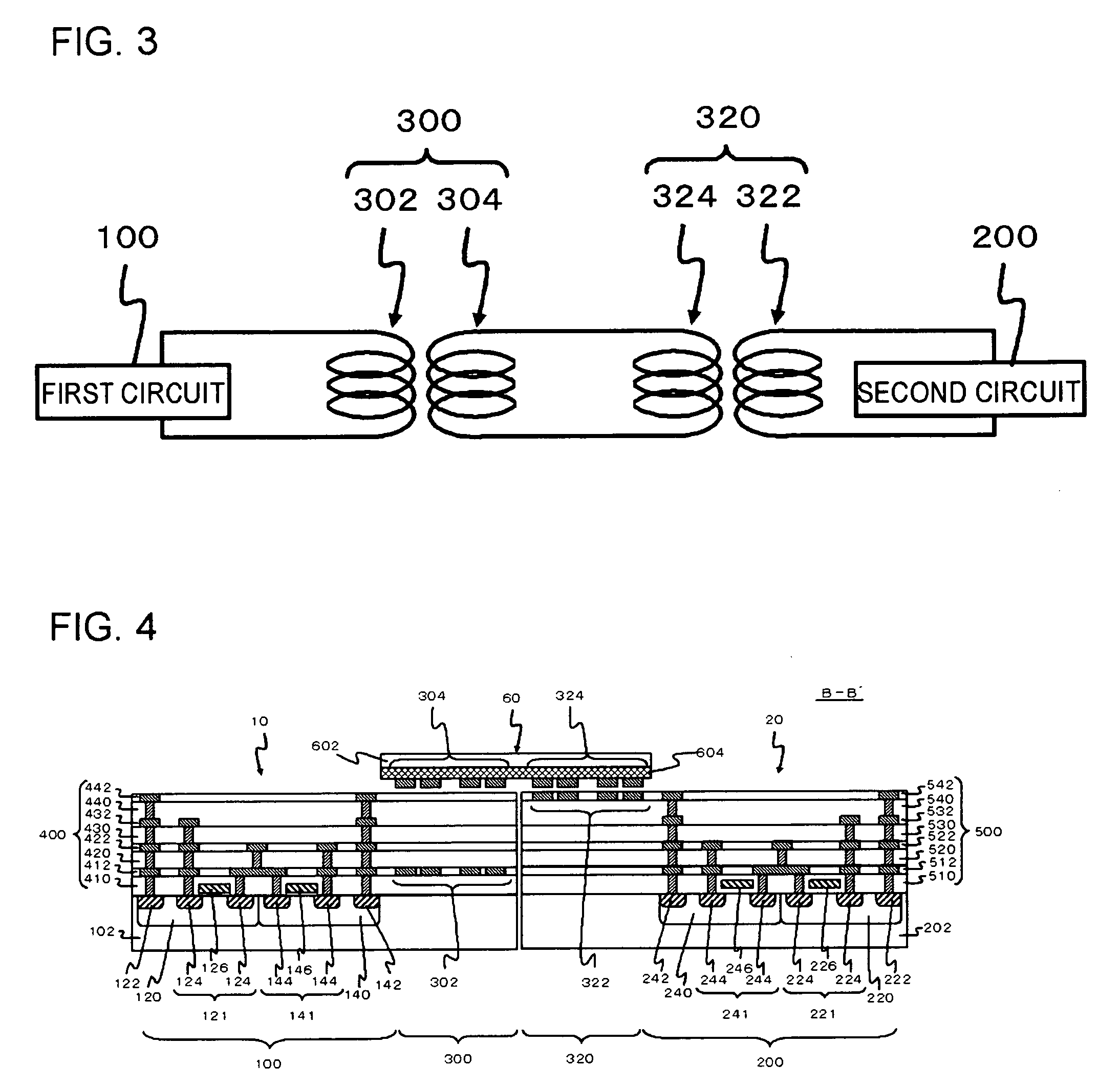
[0062]FIG. 4 is a cross-sectional view showing the structure of a semiconductor device according to a second embodiment. FIG. 5 is a schematic plan view of the semiconductor device shown in FIG. 4. FIG. 4 is a cross-sectional view of the semiconductor device, taken along the line B-B′ of FIG. 5. This semiconductor device has the same structure as the semiconductor device according to the first embodiment, except that the third inductor 304 and the fourth inductor 324 are formed on the face of the interconnect substrate 60 that faces the semiconductor chip 10 and the semiconductor chip 20.

[0063]According to this embodiment, insulation between the first circuit 100 and the second circuit 200 can also be secured while signals are being transferred with precision. Further, the fourth inductor 324 is formed on the face of the interconnect substrate 60 facing the semiconductor chip 20. With this arrangement, the distance between the fourth inductor 324 and the second inductor 322 is short...

third embodiment

[0064]FIG. 6 is a schematic cross-sectional view showing the structure of a semiconductor device according to a third embodiment. FIG. 7 is a schematic plan view of the semiconductor device shown in FIG. 6. FIG. 6 is a cross-sectional view of the semiconductor device, taken along the line C-C′ of FIG. 7. This semiconductor device has the same structure as the semiconductor device according to the first embodiment, except that a transmission / reception circuit 606 is formed in the face of the silicon substrate 602 having the interconnect layer 604 formed thereon.

[0065]FIG. 8 is an equivalent circuit diagram of the semiconductor device shown in FIGS. 6 and 7. The transmission / reception circuit 606 is provided between the third inductor 304 and the fourth inductor 324 in the circuit diagram. The transmission / reception circuit 606 includes a reception circuit and a transmission circuit. After demodulating a signal received by the third inductor 304 from the first inductor 302, the transm...


PUM


Abstract

An interconnect substrate is placed over a first inductor of a semiconductor chip and a second inductor of another semiconductor chip. The interconnect substrate includes a third inductor and a fourth inductor. The third inductor is located above the first inductor. The distance from the first inductor to the third inductor is longer than the distance from the second inductor to the fourth inductor.

Description

[0001]This application is based on Japanese patent application No. 2009-102278, the content of which is incorporated herein by reference.BACKGROUND[0002]1. Technical Field[0003]The present invention relates to a semiconductor device that is capable of transferring electric signals between two circuits to which electric signals having different potentials from each other are input.[0004]2. Related Art[0005]To transfer electric signals between two circuits to which electric signals having different potentials from each other are input, photo couplers are often used. Each photo coupler includes a light emitting element such as a light emitting diode and a light receiving element such as a photo transistor. The light emitting element converts an input electric signal into light, and the light receiving element returns the light to an electric signal. In this manner, photo couplers transfer electric signals.[0006]However, it is difficult to reduce the size of each photo coupler due to th...

Claims


Application Information

Patent Timeline
IPC IPC(8): H01L23/538
CPCH01L23/48H01L23/5227H01L23/538H01L23/645H01L2924/0002H01L25/0655H01L2924/00
Inventor NAKASHIBA, YASUTAKA
Owner RENESAS ELECTRONICS CORP
Why Eureka
Try Eureka