

Packaged electronic device having metal comprising self-healing die attach material
a technology of self-healing and die-attaching material, which is applied in the direction of semiconductor devices, semiconductor device details, electrical apparatus, etc., can solve the problems of package related failure of msl testing, loss of strength of die-attaching material, increase in cracking, etc., and achieves higher electrical and thermal conductivity, more metal content, and metal-to-metal contact area.
Active Publication Date: 2010-10-21
TEXAS INSTR INC
View PDF5 Cites 16 Cited by
- Summary
- Abstract
- Description
- Claims
- Application Information
AI Technical Summary
Benefits of technology
The patent describes a new method for attaching electronic components to a circuit board using a special adhesive. The adhesive contains metal particles and microcapsules filled with a polymerizable material and a polymerization agent. When the adhesive is compressed, the metal particles come into contact with each other, causing the polymerizable material to solidify and bind the metal particles together. This new method allows for higher metal content in the adhesive, resulting in better electrical and thermal conductivity. It also reduces the amount of polymer needed, which leads to lower costs and improved performance. The method involves introducing the adhesive between the electronic component and the circuit board, and then applying force to rupture the microcapsules and bind the metal particles together. This new method is particularly useful for high-performance electronic components that require better grounding and heat transfer.
Problems solved by technology
The amount of silver is generally limited to about 80% by volume, because a silver content above this limit is well known to result in a loss of strength of the die attach material, and as a result an increase in cracking.
Although improvements in IC mold compounds and die attach materials have enabled improved MSL classifications at higher temperatures, stress-induced delamination and cracking of the die attach adhesive, which is typically in the thermal path under the IC die, is generally the leading package related failure for MSL testing.
Delamination along surface breaking features is also known to be a reliability problem.
Being unrepairable, delamination and cracking can lower package yield, and can also lead to field (e.g. reliability) failures.
%) that is required to maintain the required strength of the die attach material, which thus limits the obtainable electrical and thermal conductivity of the die attach adhesive.
%, and thus the obtainable electrical and thermal conductivity is limited.
Being formed from a liquid resin (monomer), there is difficulty in obtaining a uniform polymer distribution which generally leads to significant polymer segregation which results in a need for conventional die attach materials to include even more % polymer.
Method used
View moreImage
Smart ImageViewing Examples

Examples
examples
[0029]Embodiments of the present invention are further illustrated by the following specific Example, which should not be construed as limiting the scope or content of embodiments of the invention in any way. A 48PHP package (7×7×1 mm HTQFP) with a 25 μm BLT, compacted to a metal density of ˜95% can be expected to have θJp values of between 0.5 and 0.3° C. / watt with embodiments of the invention, whereas values of between 1.6 and 0.7° C. / watt are generally achieved by conventional die attach materials. The metal composition for this example was silver flakes and lead / 5% tin balls.
Login to View More PUM
 Abstract
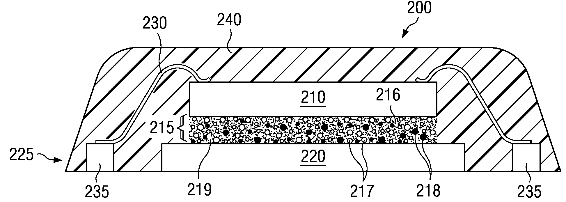
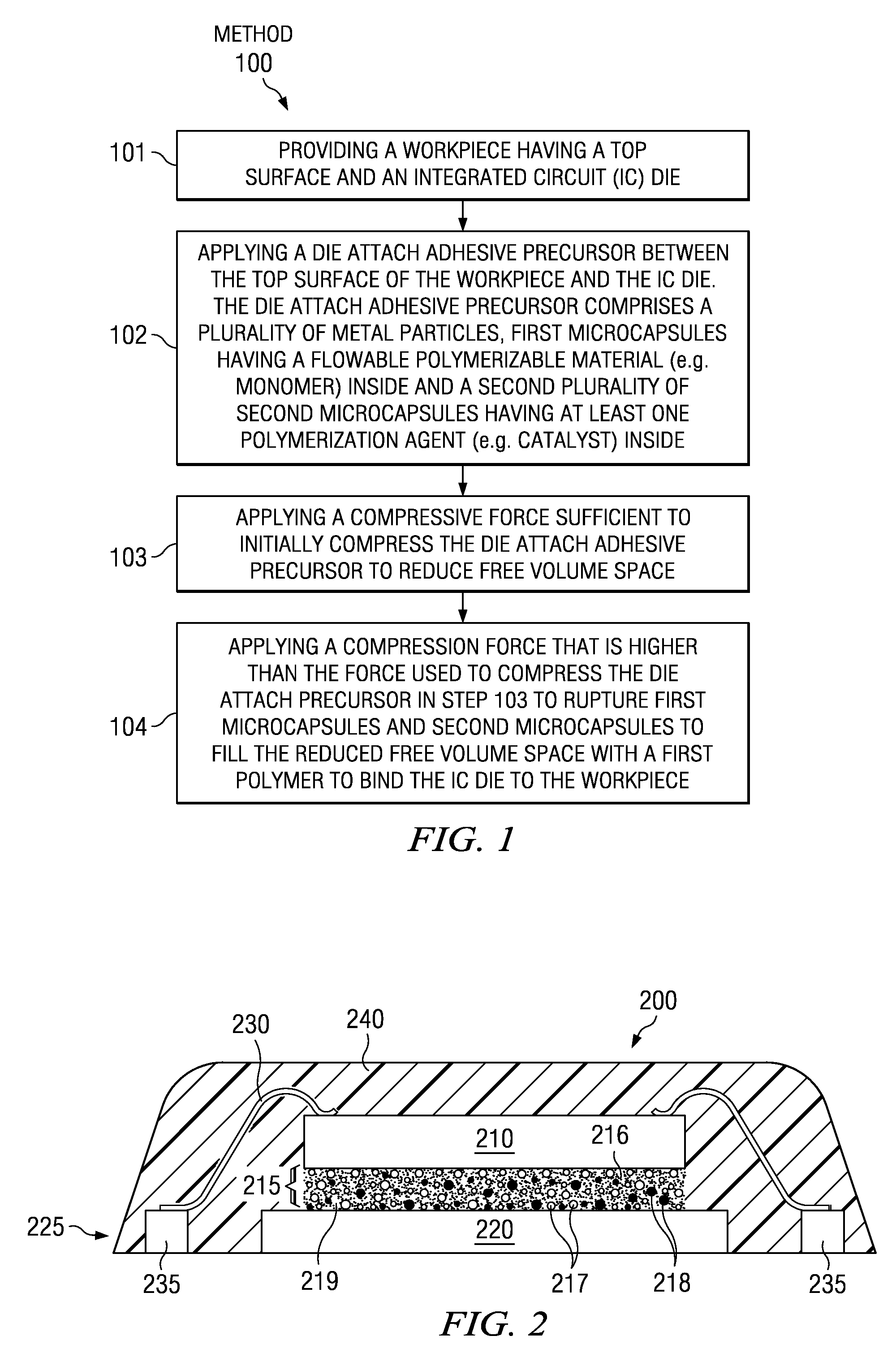
A method of assembling an electronic device and electronic packages therefrom. A die attach adhesive precursor is placed between a top surface of a workpiece and an IC die. The die attach adhesive precursor includes metal particles, a first plurality of first microcapsules having a polymerizable material inside, and a second plurality of second microcapsules having a polymerization agent inside to form a first polymer upon rupture of first and second microcapsules. A force sufficient to rupture at least a portion of the first plurality of first microcapsules and at least a portion of the second plurality of second microcapsules is applied to form a self-healing die attach adhesive wherein the first polymer binds the plurality of metal particles and the remaining microcapsules and secures the IC die to the top surface of the workpiece. The self-healing die attach adhesive generally includes at least 90 vol. % metal.
Description
FIELD OF THE INVENTION[0001]Embodiments of the present invention relate to packaged integrated circuits (IC) devices.BACKGROUND[0002]Packaged semiconductor devices generally comprise an IC die that is mounted on the die pad of a lead frame using a die attach adhesive. The die attach adhesive provides mechanical attachment, and generally also provides an electrical and / or thermal pathway to the die pad.[0003]The die attach adhesive is generally a polyimide or epoxy based adhesive. Silver is often added in particle flake form as a filler to raise both the electrical and thermal conductivity of the material. The amount of silver is generally limited to about 80% by volume, because a silver content above this limit is well known to result in a loss of strength of the die attach material, and as a result an increase in cracking.[0004]One reliability test for packaged ICs is Moisture Sensitivity Level (MSL) testing, which is used to establish floor life exposure and reflow condition limit...
Claims
Login to View More Application Information
Patent Timeline
 Patent Type & AuthorityApplications(United States)
IPC IPC(8): H01L23/48H01L21/50
CPCH01L24/29H01L24/32H01L2224/32245H01L2224/48091H01L2224/48247H01L2224/48472H01L2224/73265H01L2924/01005H01L2924/01013H01L2924/01029H01L2924/01047H01L2924/0105H01L2924/01074H01L2924/01079H01L2924/01082H01L2924/14H01L2924/0132H01L2224/29H01L2224/2919H01L2924/01006H01L2924/01019H01L2924/01033H01L2924/0665H01L2224/29366H01L2224/29384H01L2224/29324H01L2224/2929H01L2224/29311H01L2224/29339H01L2224/29347H01L2224/29355H01L2924/00013H01L2224/29298H01L2224/29499H01L2924/00014H01L2924/00012H01L2924/00H01L2924/01022H01L2924/01028H01L2924/3512H01L2224/29099H01L2224/29199H01L2224/29299H01L2924/181H01L24/73
InventorWAINERDI, JAMES C.TELLKAMP, JOHN P.
OwnerTEXAS INSTR INC