Formation of Shallow Trench Isolation Using Chemical Vapor Etch

a technology of chemical vapor etching and shallow trench isolation, which is applied in the direction of individual semiconductor device testing, semiconductor/solid-state device testing/measurement, instruments, etc., can solve the problem that the conventional process is not capable of precisely controlling the height of the fins

Inactive Publication Date: 2010-10-21
TAIWAN SEMICON MFG CO LTD
View PDF25 Cites 20 Cited by
  • Summary
  • Abstract
  • Description
  • Claims
  • Application Information

AI Technical Summary

Benefits of technology

[0012]In some embodiments, a method comprises measuring a depth of a shallow trench isolation (STI) region below a surface of a substrate. The STI region is filled with an oxide material, the substrate having a pad nitride layer above the surface. A thickness of the pad nitride layer is measured. A first chemical vapor etch of the oxide material is performed, to partially form a recess in the STI region, such that the first chemical vapor etch removes an amount of the oxide material less than the measured thickness of the pad nitride layer. The nitride layer is removed using a dry etch. A total remaining height of the STI region is measured after removing the pad nitride layer. A second chemical vapor etch of the oxide material in the STI region is performed, based on the measured depth and the total remaining height, so as to form at least one fin having a desired fin height above the oxide material in the STI region.

Problems solved by technology

There are two issues associated with the traditional bulk fin formation: (1) the conventional process is not capable of precisely controlling the height of fins 140, and (2) formation of oxide fence 132 on the bottom of fin sidewall.

Method used


Image

  • Formation of Shallow Trench Isolation Using Chemical Vapor Etch
  • Formation of Shallow Trench Isolation Using Chemical Vapor Etch
  • Formation of Shallow Trench Isolation Using Chemical Vapor Etch

Examples


Embodiment Construction

[0018]This description of the exemplary embodiments is intended to be read in connection with the accompanying drawings, which are to be considered part of the entire written description. Terms concerning attachments, coupling and the like, such as “connected” and “interconnected,” refer to a relationship wherein structures are secured or attached to one another either directly or indirectly through intervening structures, as well as both movable or rigid attachments or relationships, unless expressly described otherwise.

[0019]This disclosure provides an innovative method for precise fin formation control. Also, an integrated etch module design is disclosed with on-board metrology for closed-loop automated process control (APC) setup.

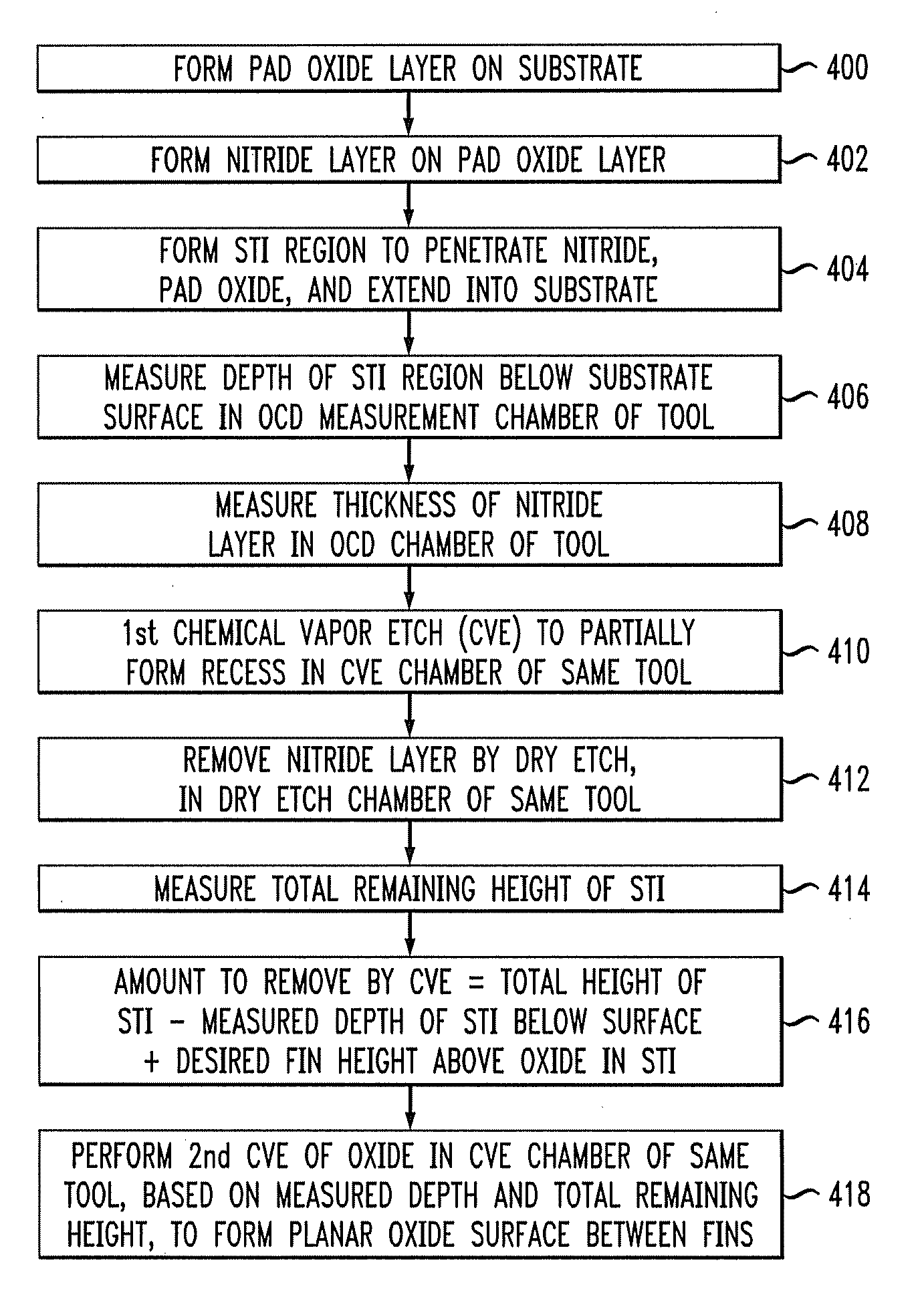
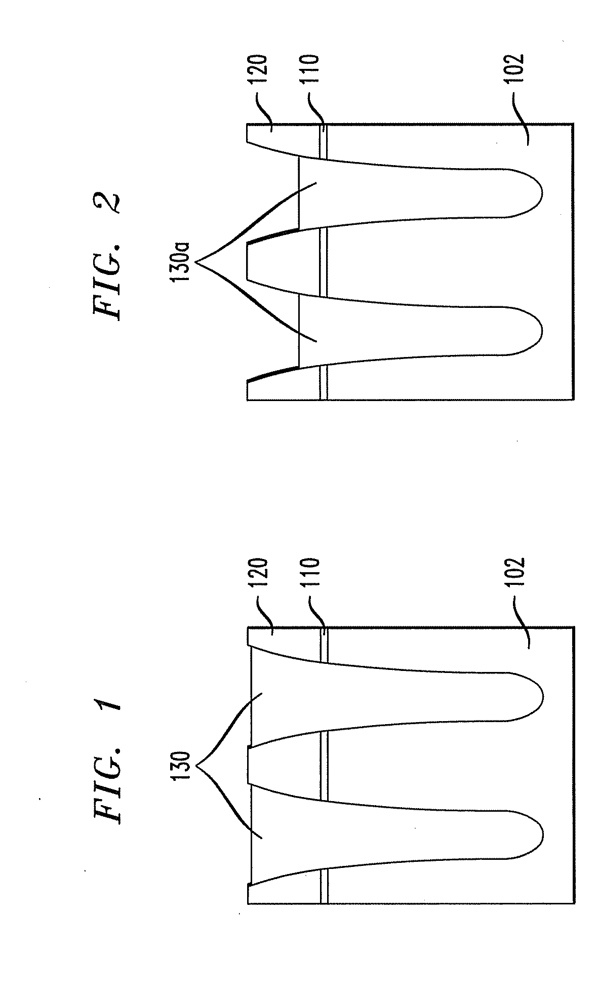
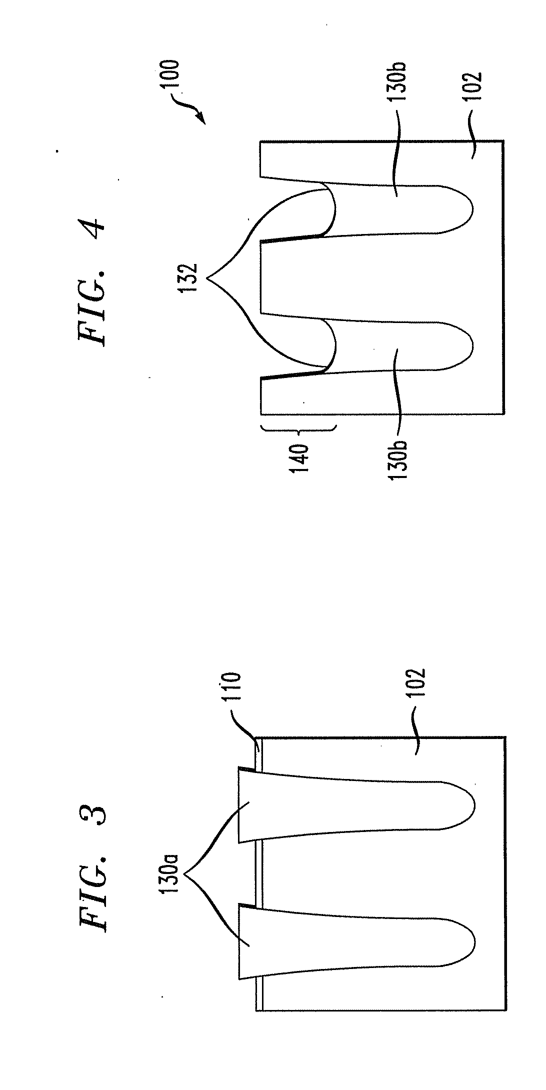
[0020]FIG. 9 shows an exemplary structure 300 including an STI region 330b with fins 340, which may be used in a FinFET, for example. FIGS. 6-9 show various stages of an exemplary process for forming the structure 300. FIG. 10 is a flow chart of an exem...


PUM

PropertyMeasurementUnit
heightaaaaaaaaaa
depthaaaaaaaaaa
heightaaaaaaaaaa

Abstract

A method includes measuring a depth of a shallow trench isolation (STI) region below a surface of a substrate. The STI region is filled with an oxide material. The substrate has a nitride layer above the surface. A thickness of the nitride layer is measured. A first chemical vapor etch (CVE) of the oxide material is performed, to partially form a recess in the STI region. The first CVE removes an amount of the oxide material less than the thickness of the nitride layer. The nitride layer is removed by dry etching. A remaining height of the STI region is measured after removing the nitride. A second CVE of the oxide material in the STI region is performed, based on the measured depth and the remaining height, to form at least one fin having a desired fin height above the oxide in the STI region without an oxide fence.

Description

FIELD OF THE INVENTION[0001]The present disclosure relates to semiconductor fabrication methods and apparatus.BACKGROUND[0002]A FinFET is a field effect transistor formed on a silicon-on-insulator (SOI) or bulk silicon substrate, with a mesa like structure including fins. FIGS. 1-4 show a conventional process for forming an STI region of a FinFET 100. For the traditional bulk fin formation process flow, fin formation starts after the CMP step is performed, at least in the shallow trench isolation (STI) regions. Fin formation involves partial dry etching to form STI recesses, wet etching for STI Nitride removal, and final wet STI recess to form desired fin height.[0003]First, a dielectric layer 110 is formed on a substrate 102. In the example, the substrate is a silicon substrate, and the dielectric layer 110 is a pad oxide layer.[0004]A pad nitride layer 120 is formed over the dielectric layer.[0005]A photoresist (not shown) is formed over the nitride layer, and an etching step is p...

Claims


Application Information

Patent Timeline
Patent Type & Authority Applications(United States)
IPC IPC(8): H01L21/66C23F1/08
CPCH01L21/76224H01L22/20H01L22/12
Inventor XIAO, YINGCHERN, CHYI SHYUAN
Owner TAIWAN SEMICON MFG CO LTD
Why Eureka
Try Eureka