System and method of manufacturing a fin field-effect transistor having multiple fin heights

a technology of field-effect transistor and manufacturing method, which is applied in the field of transistors, can solve the problems of increasing the difficulty of existing finfet manufacturing process in manufacturing finfets, uneven angled implants of fins, and reducing the precision of etching of fin height and/or fin width at higher aspect ratios, so as to achieve enhanced control and increase the aspect ratio

Active Publication Date: 2015-06-11
QUALCOMM INC
View PDF10 Cites 34 Cited by
  • Summary
  • Abstract
  • Description
  • Claims
  • Application Information

AI Technical Summary

Benefits of technology

[0007]A first FinFET device and a second FinFET device may be formed from the etch stop layers and the compound layers. For example, the first FinFET device may have a first fin that is formed from regions of the second compound layer and the first compound layer via an etching process. A first region of the second etch stop layer may be patterned to form an intermediate layer that is interposed between the first fin layer and the second fin layer. A second region of the second compound layer may be patterned to from a second fin of a second FinFET. The fin of the first FinFET device may have a different fin height than the fin of the second FinFET device. By selectively etching individual fins to the first etch stop layer or to the second etch stop layer, a variety of fin heights may be formed. Because the etch stop layers regulate fin heights, increased aspect ratios (e.g., aspect ratios greater than 3) of fins may be achieved with enhanced control.
[0008]In a particular embodiment, an apparatus comprises a first fin field effect transistor (FinFET) device extending from a surface of a first etch stop layer. The apparatus also comprises a second FinFET device extending from a surface of a second etch stop layer. A first compound layer is interposed between the first etch stop layer and the second etch stop layer.
[0009]In another particular embodiment, a method comprises forming a first fin field effect transistor (FinFET) device that extends from a surface of a first etch stop layer. The method also comprises forming a second FinFET device that extends from a surface of a second etch stop layer. A first compound layer is interposed between the first etch stop layer and the second etch stop layer.

Problems solved by technology

Existing FinFET manufacturing processes have difficulty manufacturing FinFETs with an aspect ratio (a ratio between fin height and fin width) greater than three due to imprecise etching.
Further, when the aspect ratio is greater than three, angled implants of the fin become uneven.
Some limiting factors include precision of etching of the fin height and / or fin width, decreasing implant angles at higher aspect ratios, and leakage current control at greater aspect ratios.
Designing a circuit using FinFETs with limited aspect ratios may reduce design options as compared to a design using FinFETs with a greater range of aspect ratios.

Method used


Image

  • System and method of manufacturing a fin field-effect transistor having multiple fin heights
  • System and method of manufacturing a fin field-effect transistor having multiple fin heights
  • System and method of manufacturing a fin field-effect transistor having multiple fin heights

Examples


Embodiment Construction

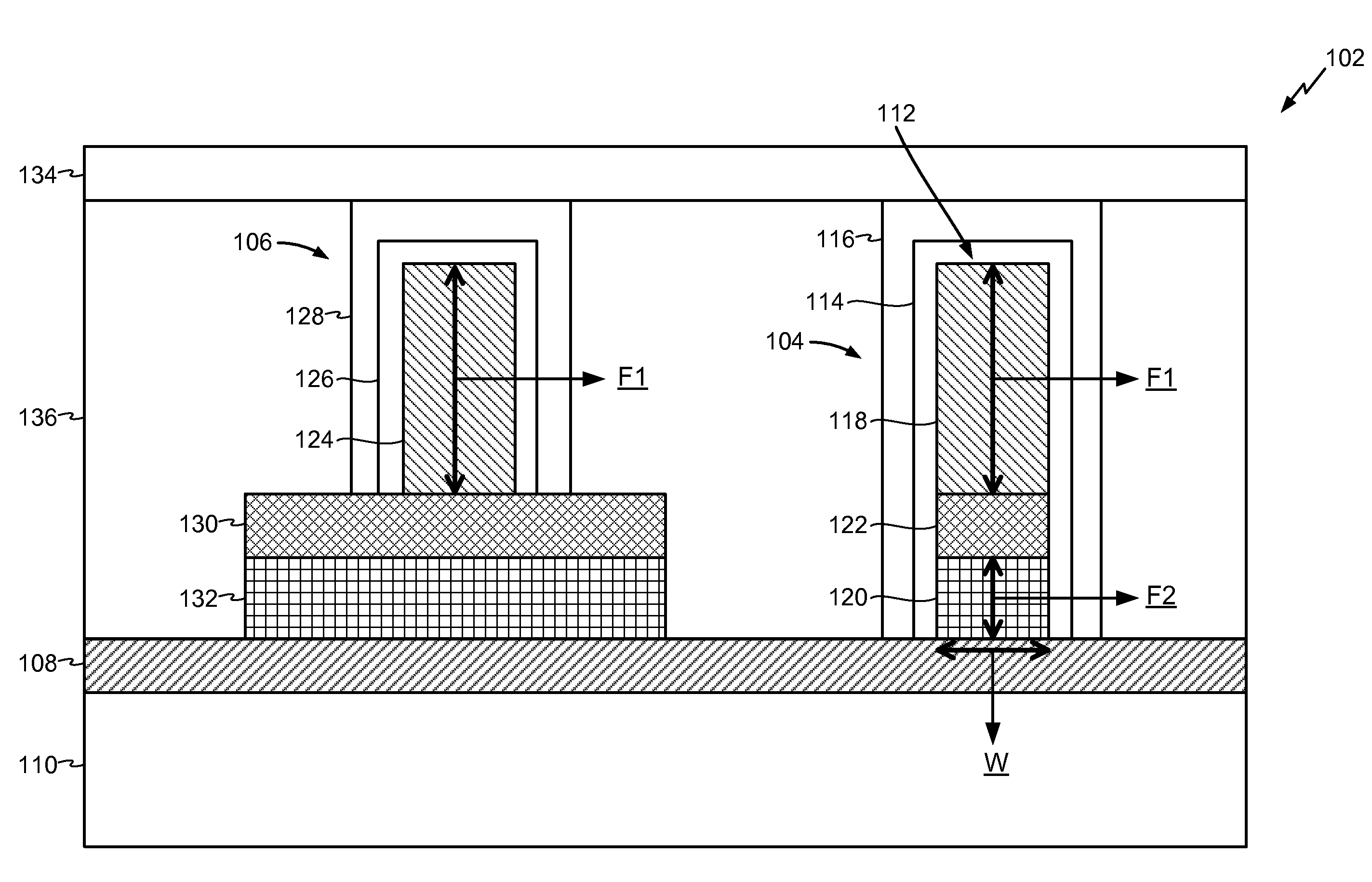
[0017]FIG. 1 is a diagram of a particular illustrative embodiment of a fin-type semiconductor device 102 (e.g., a Fin field-effect transistor (FinFET)) with fins having different effective fin heights. The fin-type semiconductor device 102 may include a first etch stop layer 108 that is formed on a surface of a substrate 110. The fin-type semiconductor device 102 may also include a first FinFET 104 and a second FinFET 106. The first FinFET 104 and the second FinFET 106 may be located within an interlayer dielectric (ILD) layer 136. The first FinFET 104 and the second FinFET 106 may be adjacent to a capacitive film layer 134.

[0018]The first FinFET 104 may extend from a surface of the first etch stop layer 108. The first FinFET 104 may include a plurality of components. For example, the first FinFET 104 may include a first fin 112, a first oxide layer 114, and a first metal gate 116. The first fin 112 may include a first fin layer 118, a second fin layer 120, and an intermediate layer...


PUM

PropertyMeasurementUnit
aspect ratiosaaaaaaaaaa

Abstract

An apparatus comprises a first fin field effect transistor (FinFET) device extending from a surface of a first etch stop layer. The apparatus also comprises a second FinFET device extending from a surface of a second etch stop layer. A first compound layer is interposed between the first etch stop layer and the second etch stop layer.

Description

I. FIELD[0001]The present disclosure is generally related to transistors.II. DESCRIPTION OF RELATED ART[0002]Advances in technology have resulted in smaller and more powerful computing devices. For example, there currently exist a variety of portable personal computing devices, including wireless computing devices, such as portable wireless telephones, personal digital assistants (PDAs), and paging devices that are small, lightweight, and easily carried by users. More specifically, portable wireless telephones, such as cellular telephones and internet protocol (IP) telephones, can communicate voice and data packets over wireless networks. Further, many such wireless telephones include other types of devices that are incorporated therein. For example, a wireless telephone can also include a digital still camera, a digital video camera, a digital recorder, and an audio file player. Also, such wireless telephones can process executable instructions, including software applications, suc...

Claims


Application Information

Patent Timeline
Patent Type & Authority Applications(United States)
IPC IPC(8): H01L29/06H01L29/22H01L29/20H01L29/78H01L29/66
CPCH01L29/0684H01L29/0657H01L29/22H01L29/66795H01L29/20H01L29/785H01L21/823431H01L27/0886
Inventor YANG, BINLI, XIACHIDAMBARAM, PRYEAP, CHOH FEI
Owner QUALCOMM INC
Why Eureka
Try Eureka