Transistor structure with high reliability and method for manufacturing the same

a transistor and high reliability technology, applied in the direction of transistors, electrical devices, semiconductor devices, etc., can solve the problems of high trap density, inability to use near the channel regions of mos devices, and limited further lowering of the eot of the gate dielectric, so as to achieve high reliability and increase current velocity

Inactive Publication Date: 2010-10-28
INOTERA MEMORIES INC
View PDF7 Cites 1 Cited by
  • Summary
  • Abstract
  • Description
  • Claims
  • Application Information

AI Technical Summary

Benefits of technology

[0008]In view of the aforementioned issues, the present invention provides a transistor structure with high reliability and a method for manufacturing the same. The prevent invention can manufacture a solid ozone boundary layer with high concentration in order to increase current velocity from a source electrode to a drain electrode.
[0009]To achieve the above-mentioned objectives, the present invention provides a transistor structure with high reliability, including: a substrate unit, a solid ozone boundary layer, a gate oxide layer and a gate electrode. In addition, the substrate unit has a substrate body, a source electrode exposed on a top surface of the substrate body, and a drain electrode exposed on the top surface of the substrate body and separated from the source electrode by a predetermined distance. The solid ozone boundary layer is gradually grown on the top surface of the substrate body by continually mixing gaseous ozone into deionized water under 40˜95□, and the solid ozone boundary layer is formed between the source electrode and the drain electrode and formed on the substrate body. The gate oxide layer is formed on a top surface of the solid ozone boundary layer. The gate electrode is formed on a top surface of the gate oxide layer.
[0010]To achieve the above-mentioned objectives, the present invention provides a method for manufacturing a transistor structure with high reliability, including: providing a substrate unit, and the substrate unit having a substrate body, a source electrode exposed on a top surface of the substrate body, and a drain electrode exposed on the top surface of the substrate body and separated from the source electrode by a predetermined distance; continually pouring deionized water on the top surface of the substrate unit; continually mixing gaseous ozone into the deionized water under 40˜95□; gradually forming a solid ozone layer on the top surface of the substrate unit by the above-mentioned mixture of the gaseous ozone and the deionized water; forming a gate oxidation material layer on a top surface of the solid ozone layer; forming a gate electrode material layer on a top surface of the gate oxidation material layer; and then removing one part of the solid ozone layer, one part of the gate oxidation material layer and one part of gate electrode material layer that are formed above the source electrode and the drain electrode in order to respectively form a solid ozone boundary layer between the source electrode and the drain electrode and on the substrate body, a gate oxide layer being formed on a top surface of the solid ozone boundary layer, and a gate electrode being formed on a top surface of the gate oxide layer.
[0011]To achieve the above-mentioned objectives, the present invention provides a method for manufacturing a transistor structure with high reliability, including: providing a substrate unit, and the substrate unit having a substrate body, a source electrode exposed on a top surface of the substrate body, and a drain electrode exposed on the top surface of the substrate body and separated from the source electrode by a predetermined distance; continually pouring deionized water on the top surface of the substrate unit; continually mixing gaseous ozone into the deionized water under 40˜95□; gradually forming a solid ozone layer on the top surface of the substrate unit by the above-mentioned mixture of the gaseous ozone and the deionized water; removing one part of the solid ozone layer to reduce the thickness of the solid ozone layer in order to form a thin solid ozone layer; forming a gate oxidation material layer on a top surface of the thin solid ozone layer; forming a gate electrode material layer on a top surface of the gate oxidation material layer; and then removing one part of the thin solid ozone layer, one part of the gate oxidation material layer and one part of gate electrode material layer that are formed above the source electrode and the drain electrode in order to respectively form a thin solid ozone boundary layer between the source electrode and the drain electrode and on the substrate body, a gate oxide layer being formed on a top surface of the thin solid ozone boundary layer, and a gate electrode being formed on a top surface of the gate oxide layer.
[0012]Therefore, the prevent invention can manufacture the solid ozone boundary layer with high concentration by matching the two steps of “continually mixing gaseous ozone into the deionized water under 40˜95□” and “gradually forming a solid ozone layer on the top surface of the substrate unit by the above-mentioned mixture of the gaseous ozone and the deionized water” in order to increase current velocity from the source electrode to the drain electrode. Hence, the present invention can generate the following advantages: (1) low roughness (RMS) on silicon surface, (2) high density oxide interface, (3) low silicon loss, (4) excellent gate oxide reliability and (5) high efficiency particle removal rate.

Problems solved by technology

High-k dielectric materials, however, have high trap densities, and thus cannot be used close to the channel regions of the MOS devices.
Further lowering of the EOT of the gate dielectric, however, has been limited, mainly due to the thickness of the base oxide layer.
This is because although reducing the thickness of the base oxide layer can cause the reduction of the EOT, as is commonly perceived, further reduction of the thickness of the base oxide is not feasible.
However, the current velocity (e−) from the source electrode 11 to the drain electrode 12 always cannot be increased effectively by using the simple transistor structure of the prior art.
In addition, the simple transistor structure of the prior art has the following deficiencies: (1) poor roughness (RMS) on silicon surface, (2) low density oxide interface, (3) high silicon loss, (4) poor gate oxide reliability, and (5) poor efficiency particle removal rate.

Method used


Image

  • Transistor structure with high reliability and method for manufacturing the same
  • Transistor structure with high reliability and method for manufacturing the same
  • Transistor structure with high reliability and method for manufacturing the same

Examples


first embodiment

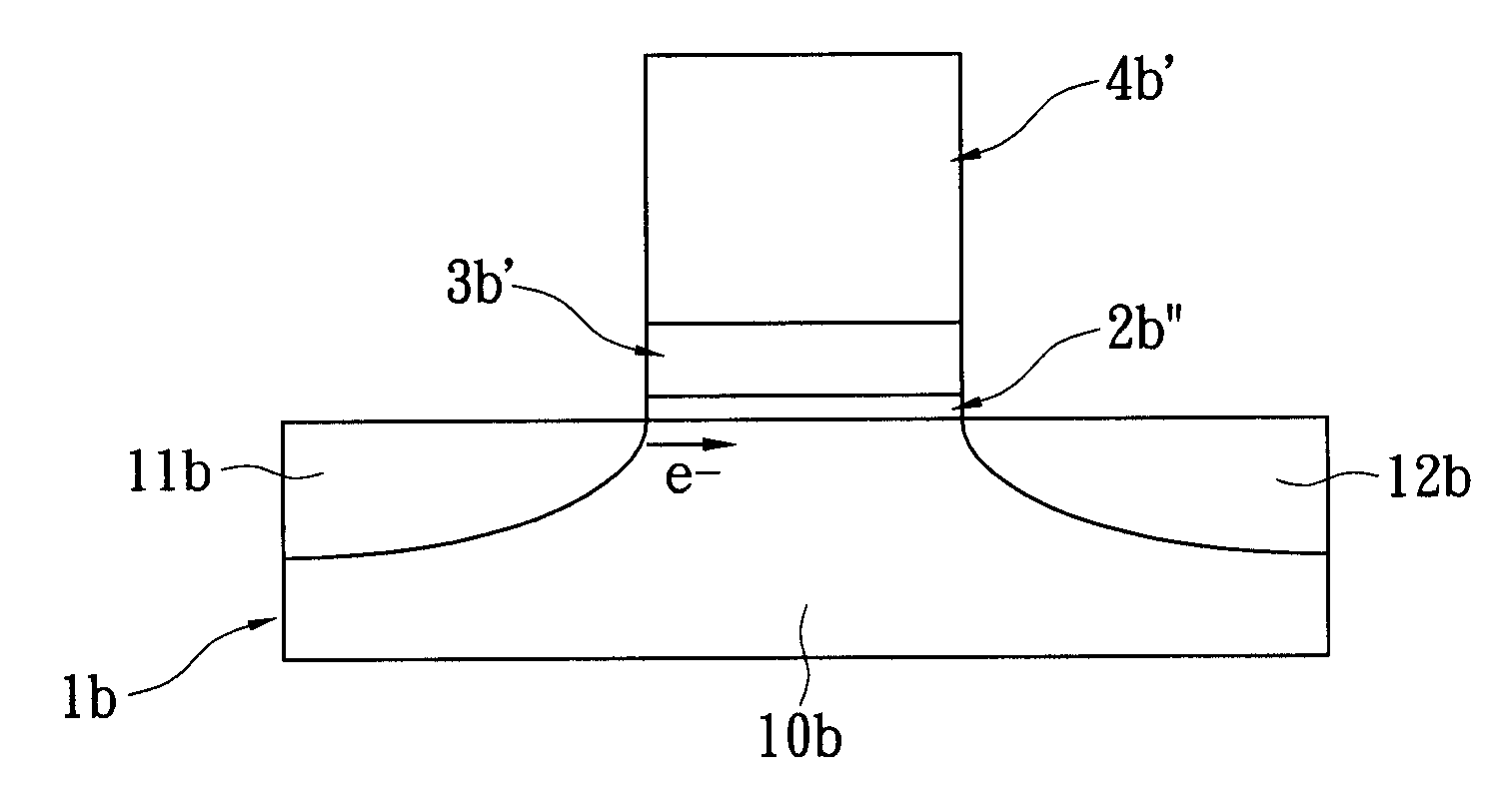
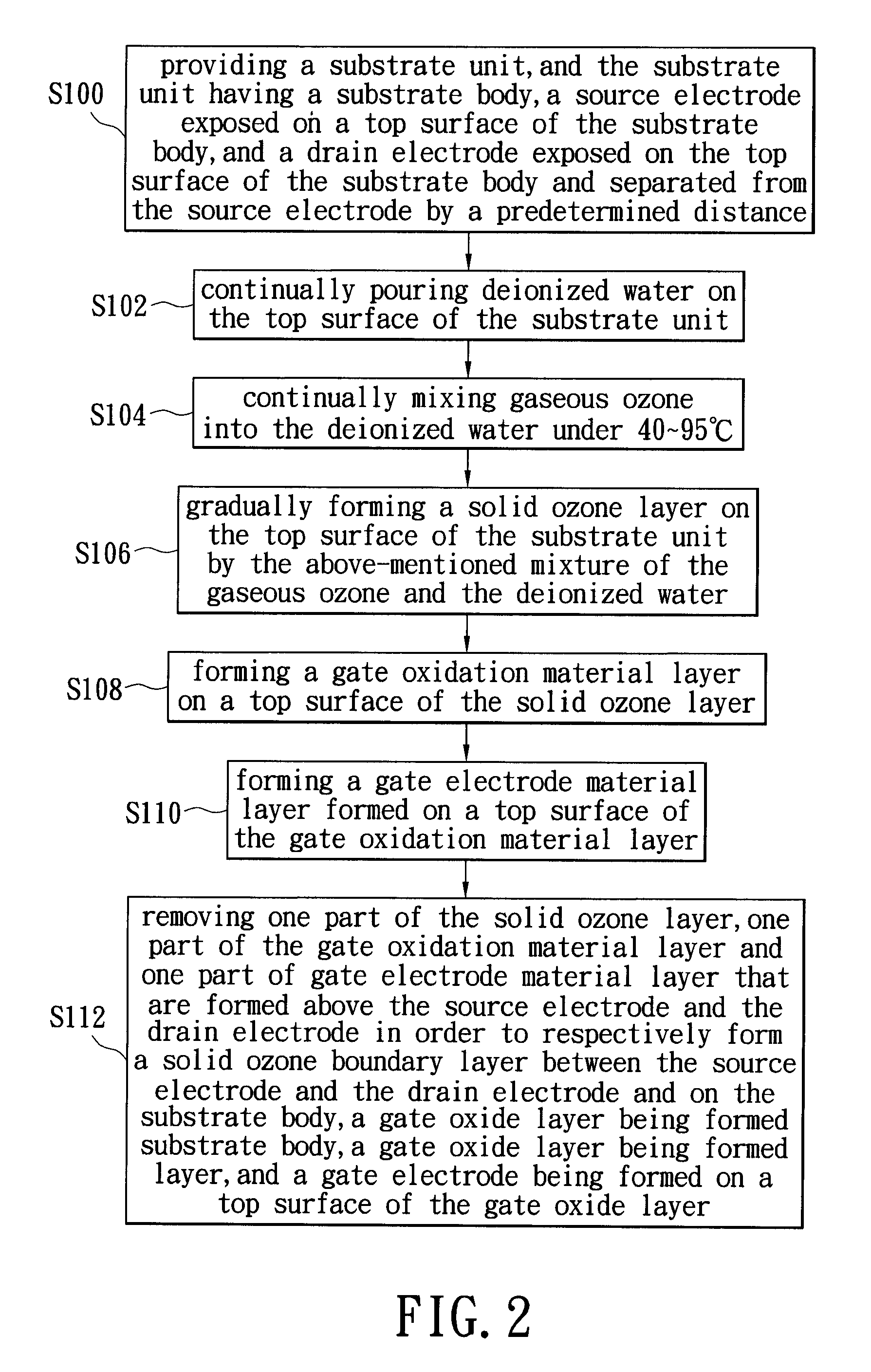
[0033]Referring to FIG. 2, the present invention provides a method for manufacturing a transistor structure with high reliability. The method includes the following steps: providing a substrate unit; continually pouring deionized water on the top surface of the substrate unit; continually mixing gaseous ozone into the deionized water under 40˜95□; gradually forming a solid ozone layer on the top surface of the substrate unit by the above-mentioned mixture of the gaseous ozone and the deionized water; forming a gate oxidation material layer on a top surface of the solid ozone layer; forming a gate electrode material layer on a top surface of the gate oxidation material layer; and then removing one part of the solid ozone layer, one part of the gate oxidation material layer and one part of gate electrode material layer that are formed above a source electrode and a drain electrode of the substrate unit.

[0034]Referring to FIGS. 2A to 2D, the detail description of the first embodiment i...

second embodiment

[0043]Referring to FIG. 3, the present invention provides a method for manufacturing a transistor structure with high reliability. The method includes the following steps: providing a substrate unit; continually pouring deionized water on the top surface of the substrate unit; continually mixing gaseous ozone into the deionized water under 40˜95□; gradually forming a solid ozone layer on the top surface of the substrate unit by the above-mentioned mixture of the gaseous ozone and the deionized water; removing one part of the solid ozone layer to reduce the thickness of the solid ozone layer in order to form a thin solid ozone layer; forming a gate oxidation material layer on a top surface of the thin solid ozone layer; forming a gate electrode material layer on a top surface of the gate oxidation material layer; and then removing one part of the thin solid ozone layer, one part of the gate oxidation material layer and one part of gate electrode material layer that are formed above a...


PUM


Abstract

A transistor structure with high reliability includes a substrate unit, a solid ozone boundary layer, a gate oxide layer and a gate electrode. In addition, the substrate unit has a substrate body, a source electrode exposed on a top surface of the substrate body, and a drain electrode exposed on the top surface of the substrate body and separated from the source electrode by a predetermined distance. The solid ozone boundary layer is gradually grown on the top surface of the substrate body by continually mixing gaseous ozone into deionized water under 40˜95□, and the solid ozone boundary layer is formed between the source electrode and the drain electrode and formed on the substrate body. The gate oxide layer is formed on a top surface of the solid ozone boundary layer. The gate electrode is formed on a top surface of the gate oxide layer.

Description

BACKGROUND OF THE INVENTION[0001]1. Field of the Invention[0002]The present invention relates to a transistor structure and a method for manufacturing the same, in particular, to a transistor structure with high reliability and a method for manufacturing the same.[0003]2. Description of Related Art[0004]With the scaling of integrated circuits, applications require an increasingly faster speed. This puts a requirement on the metal-oxide-semiconductor (MOS) devices, demanding that the MOS devices switch faster. As is known in the art, to increase the speed of MOS devices, high dielectric constant values (k values) of the gate dielectrics are desired. Since conventional silicon oxide, which has a k value of about 3.9, cannot satisfy such a requirement, high-k dielectric materials, which include oxides, nitrides, and oxynitrides, are increasingly used.[0005]High-k dielectric materials, however, have high trap densities, and thus cannot be used close to the channel regions of the MOS dev...

Claims


Application Information

Patent Timeline
Patent Type & Authority Applications(United States)
IPC IPC(8): H01L29/78H01L21/28H01L21/336
CPCH01L21/28211H01L29/78H01L29/6659H01L29/51
Inventor KUO, CHIH-CHIANGLIN, CHIN-LIEN
Owner INOTERA MEMORIES INC
Why Eureka
Try Eureka