Output circuit using analog amplifier

Inactive Publication Date: 2010-10-28
RENESAS ELECTRONICS CORP
View PDF2 Cites 0 Cited by
  • Summary
  • Abstract
  • Description
  • Claims
  • Application Information

AI Technical Summary

Benefits of technology

[0014]According to the present invention, an output characteristic can be improved, avoiding a voltage drop by an electrostatic protection resistance due to an idling current.

Problems solved by technology

However, as a result of them, a parasitic capacitance increases, a chip size increases, or a desired characteristic cannot be accomplished.
However, when the electrostatic protection resistance is connected to the output circuit, the output characteristic reduces.
However, since the electrostatic protection resistance RESD of the resistance value determined to satisfy the standard has to be inserted actually, the output characteristic is consequently limited by the electrostatic protection resistance RESD.

Method used


Image

  • Output circuit using analog amplifier
  • Output circuit using analog amplifier
  • Output circuit using analog amplifier

Examples


first embodiment

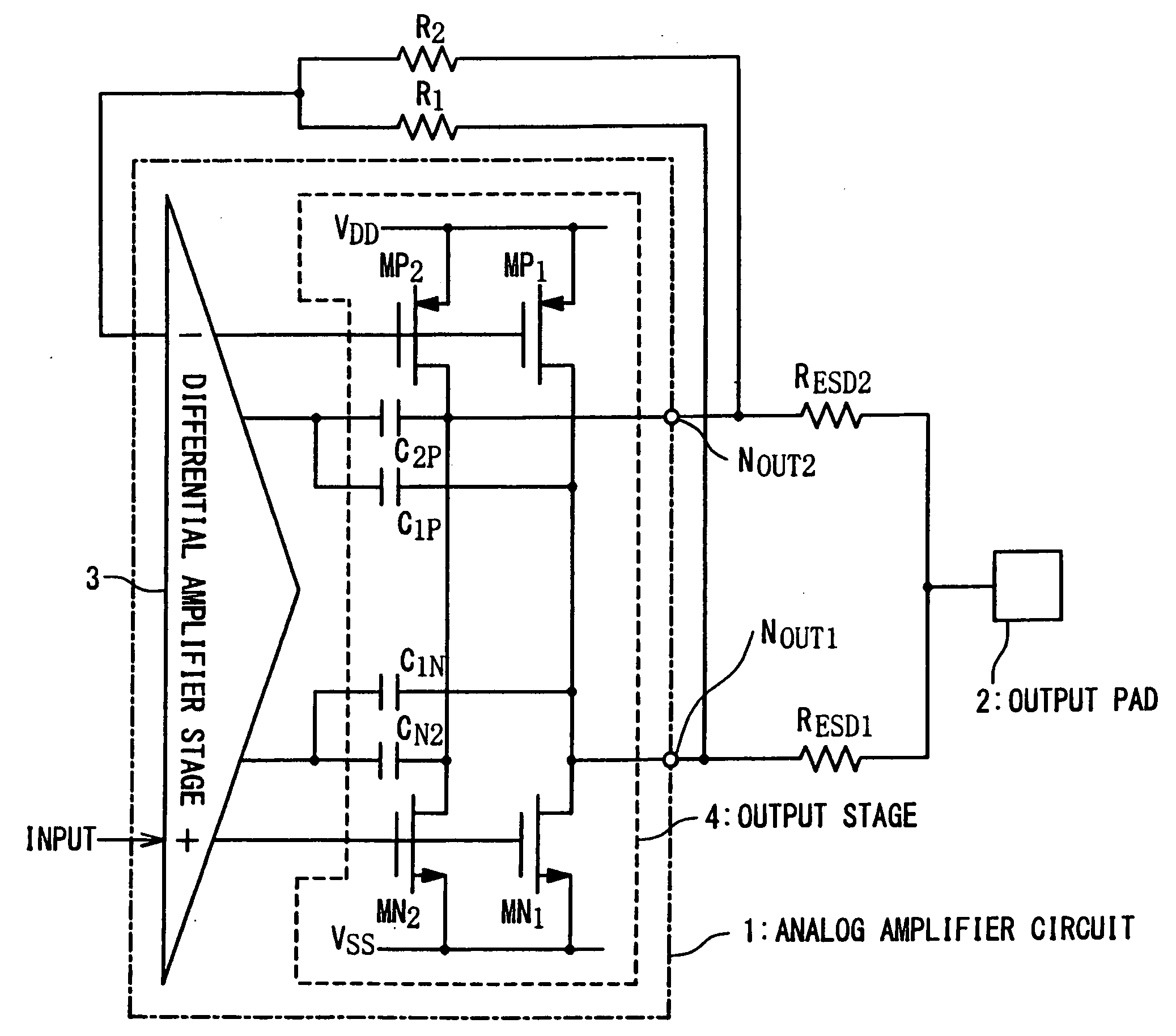
[0024]FIG. 4 is a circuit diagram showing a configuration of an output circuit according to a first embodiment of the present invention. The output circuit shown in FIG. 4 includes an analog amplifier circuit 1, an output pad 2, electrostatic protection resistances RESD1 and RESD2, and feedback resistances R1 and R2.

[0025]The analog amplifier circuit 1 includes a differential amplifier stage 3 and an output stage 4. The output stage 4 includes two output systems: one output system including a PMOS transistor MP1 and a NMOS transistor MN1 and the other output system including a PMOS transistor MP2 and a NMOS transistor MN2. In the present embodiment, the PMOS transistors MP1 and MP2 have a same W / L ratio, and the NMOS transistors MN1 and MN2 also have a same W / L ratio. Namely, the PMOS transistors MP1 and MP2 have a same driving performance, and the NMOS transistors MN1 and MN2 have a same driving performance.

[0026]Sources of the PMOS transistors MP1 and MP2 are commonly connected to...

second embodiment

[0033]FIG. 6 is a circuit diagram showing a configuration of the output circuit according to a second embodiment of the present invention. The circuit configuration shown in FIG. 6 is obtained by generalizing the circuit configuration shown in FIG. 4, and has n (n is a natural number larger than 1) output systems. The circuit configuration in FIG. 4 is the example where n=2 in FIG. 6.

[0034]Specifically, in the second embodiment, the output stage 4 of, the analog amplifier circuit 1 includes n PMOS transistors MP1 to MPn, and n NMOS transistors MN1 to MNn, and these MOS transistors constitute the n output systems. The respective sources of the PMOS transistors MP1 to MPn are commonly connected to the power supply having the positive power supply voltage VDD, and the respective gates are commonly connected to one of the outputs of the differential amplifier stage 3. Meanwhile, the respective sources of the NMOS transistors MN1 to MNn are commonly connected to the power supply having t...

third embodiment

[0037]Referring to FIG. 7, a configuration of an output circuit according to a third embodiment of the present invention will be described. In the output circuit according to the third embodiment, the feedback input point is changed from that in the first embodiment (referring to FIG. 4). Specifically, the feedback resistances R1 and R2 in FIG. 4 are removed, and instead of these elements, a third electrostatic protection resistance REDS3 is provided between the inversion input terminal of the differential amplifier stage 3 and the output pad 2. The remaining configuration is exactly the same as that in the first embodiment (FIG. 4). It should be note that a configuration in which the feedback resistances R1 to Rn are removed, one end of the third electrostatic protection resistance REDS3 is connected to the inversion input terminal of the differential amplifier stage 3, and the other end of the third electrostatic protection resistance REDS3 is connected to the output pad 2 can be ...


PUM


Abstract

An output circuit includes an analog amplifier circuit including a differential amplifier stage configured to receive an input voltage, and first to nth output systems (n is a natural number more than 1); first to nth output nodes; an output pad; and first to nth electrostatic protection resistances. An ith output system (i is a natural number between 2 and n) of the first to nth output systems includes an ith PMOS transistor having a drain connected with the ith output node of the first to nth output nodes and a gate connected with a first output of the differential amplifier stage; and an ith NMOS transistor having a drain connected with the ith output node and a gate connected with a second output of the differential amplifier stage. The first to nth electrostatic protection resistances are respectively connected between the first to nth output nodes and the output pad.

Description

INCORPORATION BY REFERENCE[0001]This application claims a priority on convention based on Japanese Patent Application No. 2009-108338. The disclosure thereof is incorporated herein by reference.TECHNICAL FIELD[0002]The present invention relates to an output circuit, and more particularly relates to a technique for reducing influence of an electrostatic protection resistance connected to a pad in an output circuit using an analog amplifier.BACKGROUND ART[0003]Generally, in an output circuit of an integrated circuit, an electrostatic protection resistance is inserted in series between an output stage and an output pad. When the electrostatic protection resistance is not inserted in series, a size of a transistor in the output stage must be increased or an output transistor must have an electrostatic protection element. However, as a result of them, a parasitic capacitance increases, a chip size increases, or a desired characteristic cannot be accomplished.[0004]When the electrostatic ...

Claims


Application Information

Patent Timeline
IPC IPC(8): H03F3/45
CPCH03F3/3022H03F3/45475H03F2203/45631H03F2203/30111H03F2203/45528H03F2203/30078
Inventor NISHIMURA, KOUICHI
Owner RENESAS ELECTRONICS CORP
Why Eureka
Try Eureka